The chip has five hardwired MSBs and takes two LSBs directly from the
input pins SB_BASE[1:0].
Bit 6, MSB
1
Bit 5
1
Bit 4
0
Bit 3
1
Bit 2
0
Bit 1
Bit 0, LSB
SB_BASE.1
SB_BASE.0
The addressing scheme in the L64777 complies with that of the LSI
Logic L64724, but, due to its small 7-bit internal address space, the
L64777 supports only group 0 and group 2. The bit location [2:0] within
the first data byte transmitted to the device specifies the group.
Group 0 is the address pointer register (APR); the Serial Control
Interface loads the following data byte to APR0. Reading or writing from
Group 2 causes a data transfer with the device address specified by
APR0:
•
If APR0 is set to zero, the Serial Control Interface expects a write
access with 196 data bytes to load the filter coefficients; it does not
apply an autoincrement to APR0.
•
If APR0 is not at zero, the Serial Control Interface expects only a
single data byte and applies an autoincrement to the APR0.
The L64777 ignores Group 1 and Groups 3 to 7. It does not apply any
reading or writing from them.
The detailed timing of the serial bus is given in Appendix A. The serial
bus is designed to run at a maximum 400 kHz clock rate. The serial
control interface can transfer reads and writes in single-byte or burst
mode. It must do read access to the status registers 12 and 13 as a
single-byte read.
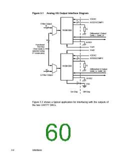
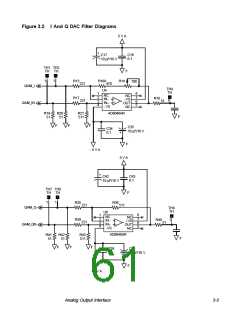
3.3 Analog Output Interface
The L64777 puts out the I and Q component of its signal on two separate
analog output interfaces (see Figure 3.1). The output interface contains
two internal 10-bit digital-to-analog converters.
Analog Output Interface
3-3

 ETC [ ETC ]