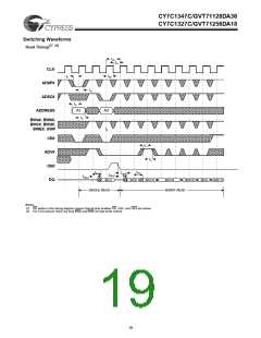
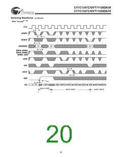
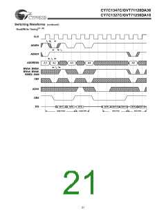
CY7C1347C/GVT71128DA36
CY7C1327C/GVT71256DA18
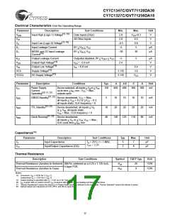
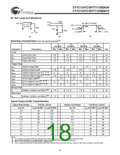
AC Test Loads and Waveforms
317
Ω
3.3V
DQ
DQ
ALL INPUT PULSES
3.0V
0V
90%
10%
Z =50
Ω
90%
0
10%
1.5 ns
50
Ω
5 pF
351
Ω
1.5 ns
≤
≤
V = 1.5V
t
(c)
(a)
(b)
[23]
Switching Characteristics Over the Operating Range
-4
250 MHz
-4.4
225 MHz
-5
200 MHz
-6
166 MHz
Parameter
Clock
Description
Min. Max. Min. Max. Min. Max. Min. Max. Unit
t
t
t
Clock Cycle Time
4.0
1.6
1.6
4.4
1.7
1.7
5.0
2.0
2.0
6.0
2.4
2.4
ns
ns
ns
KC
KH
KL
Clock HIGH Time
Clock LOW Time
Output Times
t
t
t
t
t
t
t
Clock to Output Valid
Clock to Output Invalid
Clock to Output in Low-Z
2.5
2.5
2.5
3.5
ns
ns
ns
ns
ns
ns
ns
KQ
1.25
0
1.25
0
1.25
0
1.25
0
KQX
[14, 19, 24]
[14, 19, 24]
KQLZ
KQHZ
OEQ
OELZ
OEHZ
Clock to Output in High-Z
1.25
3.0
2.5
1.25
3.0
2.5
1.25
3.0
2.5
1.25
4.0
3.5
[25]
OE to Output Valid
[14, 19, 24]
OE to Output in Low-Z
OE to Output in High-Z
0
0
0
0
[14, 19, 24]
2.5
2.5
2.5
3.5
Set-up Times
[26]
[26]
t
Address, Controls, and Data In
1.0
1.0
1.0
1.0
1.0
1.0
1.0
1.0
ns
ns
S
Hold Times
t
Address, Controls, and Data In
H
Typical Output Buffer Characteristics
Output High Voltage
(V)
Pull-Up Current
Output Low Voltage
(V)
Pull-Down Current
V
I
(mA) Min.
I
(mA) Max.
–105
–105
–105
–83
V
I
(mA) Min.
I (mA) Max.
OL
OH
OH
OH
OL
OL
–0.5
0
–38
–38
–38
–26
–20
0
–0.5
0
0
0
0
0
0.8
1.25
1.5
2.3
2.7
2.9
3.4
0.4
0.8
1.25
1.6
2.8
3.2
3.4
10
20
31
40
40
40
40
20
40
63
80
80
80
80
–70
–30
0
–10
0
0
0
0
Notes:
23. Test conditions as specified with the output loading as shown in part (a) of AC Test Loads unless otherwise noted.
24. At any given temperature and voltage condition, tKQHZ is less than tKQLZ and tOEHZ is less than tOELZ
.
25. OE is a “don’t care” when a byte write enable is sampled LOW.
26. This is a synchronous device. All synchronous inputs must meet specified set-up and hold time, except for “don’t care” as defined in the truth table.
18

 ETC [ ETC ]