Signal Description
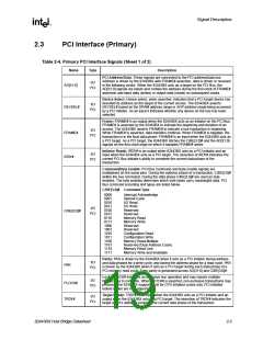
2. PCI signals are redefined when used in AGP transactions carried using AGP protocol extension. For
transactions on the AGP interface carried using PCI protocol these signals completely preserve PCI
semantics. The exact role of all PCI signals during AGP transactions is in Table 2-6.
3. The LOCK# signal is not supported on the AGP interface (even for PCI operations).
4. PCI signals described in Table 2-4 behave according to PCI 2.1 specifications when used to perform PCI
transactions on the AGP Interface.
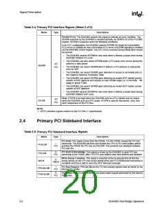
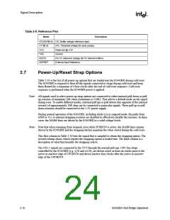
2.6
Clocks, Reset, and Miscellaneous
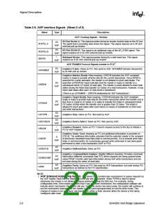
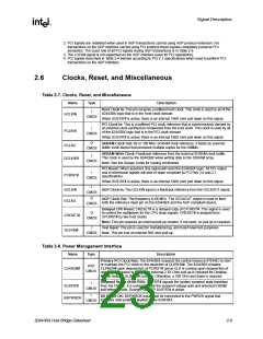
Table 2-7. Clocks, Reset, and Miscellaneous
Name
Type
Description
Host Clock In: This pin receives a buffered host clock. This clock is used by all of the
82443BX logic that is in the Host clock domain.
I
HCLKIN
CMOS
When SUSTAT# is active, there is an internal 100K ohm pull down on this signal.
PCI Clock In: This is a buffered PCI clock reference that is synchronously derived by
an external clock synthesizer component from the host clock. This clock is used by all
of the 82443BX logic that is in the PCI clock domain.
I
PCLKIN
CMOS
When SUSTAT# is active, there is an internal 100K ohm pull down on this signal.
O
SDRAM Clock Out: 66 or 100 MHz SDRAM clock reference. It feeds an external
buffer clock device that produces multiple copies for the DIMMs.
DCLKO
CMOS
SDRAM Write Clock: Feedback reference from the external SDRAM clock buffer.
This clock is used by the 82443BX when writing data to the SDRAM array.
I
DCLKWR
CMOS
Note: See the Design Guide for routing constraints.
PCI Reset: When asserted, this signal will reset the 82443BX logic. All PCI output
and bi-directional signals will also tri-state compliant to PCI Rev 2.0 and 2.1
specifications.
I
PCIRST#
CMOS
When SUSTAT# is active, there is an internal 100K ohm pull down on this signal.
I
GCLKIN
GCLKO
AGP Clock In: The GCLKIN input is a feedback reference from the GCLKOUT signal.
CMOS
O
AGP Clock Out: The frequency is 66 MHz. The GCLKOUT output is used to feed
both the reference input pin on the 82443BX and the AGP compliant device.
CMOS
Delayed CPU Reset: CRESET# is a delayed copy of CPURST#. This signal is used
to control the multiplexer for the CPU strap signals. CRESET# is delayed from
CPURST# by two host clocks.
O
CRESET#
TESTIN#
CMOS
Note: This pin requires an external pull-up resistor. If not used, no pull up is required.
Test Input: This pin is used for manufacturing, and board level test purposes.
I
CMOS Note: This pin has an internal 50K ohm pull-up.
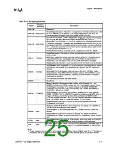
Table 2-8. Power Management Interface
Name
Type
Description
Primary PCI Clock Run: The 82443BX requests the central resource (PIIX4E) to start
or maintain the PCI clock by the assertion of CLKRUN#. The 82443BX tristates
CLKRUN# upon deassertion of PCIRST# (since CLK is running upon deassertion of
reset). If connected to PIIX4E an external 2.7K Ohm pull-up is required for Desktop,
Mobile requires (8.2k–10K) pull-up. Otherwise, a 100 Ohm pull down is required.
I/OD
CLKRUN#
CMOS
Suspend Status (from PIIX): SUSTAT# signals the system suspend state transition
from the PIIX4E. It is used to isolate the suspend voltage well and enter/exit DRAM
self-refresh mode. During POS/STR SUSTAT# is active.
I
SUSTAT#
CMOS
I
BX Power OK: BXPWROK input must be connected to the PWROK signal that
indicates valid power is applied to the 82443BX.
BXPWROK
CMOS
82443BX Host Bridge Datasheet
2-9

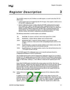
 ETC [ ETC ]