<ꢀ5ꢁꢀꢂꢃ<ꢀ.ꢁꢀꢂ
'PJCPEGFꢄ<ꢁꢀꢂꢄ/KETQRTQEGUUQT
ZiLOG
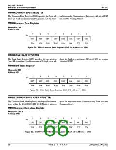
%#ꢋ %#ꢂꢅ%#ꢄꢌ$KVUꢄꢐ ꢉꢍꢆꢄ%#specifiesthestart(Low)ad-
dress (on 4-KB boundaries) for Common Area 1. This con-
dition also determines the most recent address of the Bank
Area. All bits of %# are set to 1 during 4'5'6.
$#ꢋ $#ꢂꢄꢌ$KVUꢄꢋ ꢂꢍꢆꢄ$# specifiesthe start (Low)address
(on 4-KB boundaries) for the Bank Area. This condition
also determines the most recent address of Common Area
0. All bits of $# are set to 1 during 4'5'6.
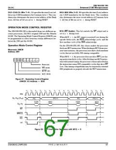
12'4#6+10ꢄ/1&'ꢄ%10641.ꢄ4')+56'4
/ꢁ'ꢄꢌ/ꢁꢄ'PCDNGꢍꢆꢄThis bit controls the /ꢄ output and is
set to a 1 during reset.
The Z8S180/Z8L180 is descended from two different an-
cestor processors, ZiLOG’s original Z80 and the Hitachi
64180. The Operating Mode Control Register (1/%4) can
be programmed to select between certain differences be-
tween the Z80 and the 64180.
When /ꢄ'ꢅꢐ 1, the /ꢄ output is asserted Low during the
opcode fetch cycle, the +06ꢀ acknowledge cycle, and the
first machine cycle of the 0/+ acknowledge.
1RGTCVKQPꢄ/QFGꢄ%QPVTQNꢄ4GIKUVGT
On the Z8S180/Z8L180, this choice makes the processor
fetch one4'6+ instruction. When fetching a4'6+ fromzero-
wait-state memory, the processor uses three clock machine
cycles that are not fully Z80-timing-compatible.
/PGOQPKEꢄ1/%4
#FFTGUUꢄꢋ'*
When /ꢄ'ꢅꢐꢅ0, the processor does not drive /ꢄ Low dur-
inginstruction fetchcycles. Afterfetchingone4'6+instruc-
tion with normal timing, the processor returns and refetches
the instruction using Z80-compatible cycles that drive /ꢄ
Low. Thistimingcompatibilitymayberequiredbyexternal
Z80 peripherals to properly decode the 4'6+ instruction.
&ꢊ &ꢁ &ꢏ
4GUGTXGF
+1%ꢅꢈ4ꢌ9ꢉ
/ꢄ6'ꢅꢈ9ꢉ
/ꢄ'ꢅꢈ4ꢌ9ꢉ
(KIWTG ꢀꢁꢆ 1RGTCVKPIꢄ%QPVTQNꢄ4GIKUVGT
ꢌ1/%4ꢅꢄ+ꢃ1ꢄ#FFTGUUꢄꢒꢄꢋ'*ꢍ
T1 T2 T3 T1 T2 T3
TI
TI
TI T1 T2 T3
TI T1 T2 T3
TI
2*+
A0–A18 (A19)
PC+1
PC
EDH
PC+1
PC
EDH
4DH
4DH
D0–D7
M1
MREQ
RD
ST
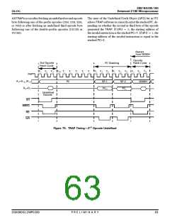
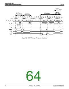
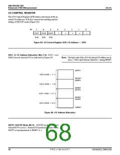
(KIWTG ꢀꢇꢆ 4'6+ꢄ+PUVTWEVKQPꢄ5GSWGPEGꢄYKVJꢄ/ꢁ'ꢄꢒꢄꢂ
&5ꢀꢀꢁꢀꢀꢂꢃ</2ꢀꢂꢀꢀ
2ꢅ4ꢅ'ꢅ.ꢅ+ꢅ/ꢅ+ꢅ0ꢅ#ꢅ4ꢅ;
ꢁꢊ

 ZILOG [ ZILOG, INC. ]