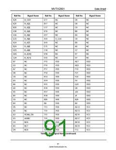
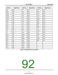
MVTX2801
Data Sheet
11.5 AC Characteristics and Timing
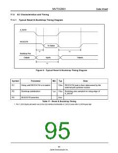
11.5.1 Typical Reset & Bootstrap Timing Diagram
S_RST#
RESOUT#
Tri-Stated
R1
R3
Bootstrap Pins
Outputs
Inputs
Outputs
R2
Figure 6 - Typical Reset & Bootstrap Timing Diagram
Symbol
Parameter
Min Typ
Note:
R1
Delay until RESOUT# is tri-stated
10ns RESOUT# state is then determined by the
external pull-up/down resistor
R2
R3
Bootstrap stabilization
1µs 10µs Bootstrap pins sampled on rising edge of
1
S_RST#
RESOUT# assertion
2ms
Table 11 - Reset & Bootstrap Timing
1. The T_D[15:0] pins will switch over to the LED interface functionality in 3 SCLK cycles after S_RST# goes high
95
Zarlink Semiconductor Inc.

 ZARLINK [ ZARLINK SEMICONDUCTOR INC ]