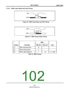
MVTX2801
Data Sheet
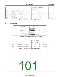
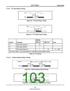
11.5.9 I2C Input Setup Timing
SCL
S1
S2
SDA
2
Figure 20 - I C Input Setup Timing
SCL
S3-max
S3-min
SDA
2
Figure 21 - I C Output Delay Timing
500KHz
Symbol
S1
Parameter
Min (ns)
Max (ns)
Note:
SDA input setup time
SDA input hold time
SDA output delay time
20
1
S2
S3
1
20
CL = 30pf
Open Drain Output. Low to High transistor is controlled by external pullup resistor.
2
Table 19 - I C Timing
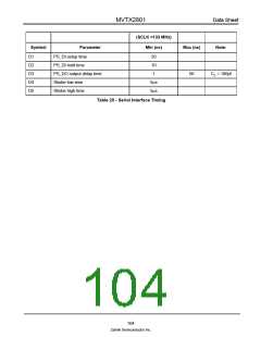
11.5.10 Serial Interface Setup Timing
STROBE
PS_DI
D4
D5
D1
D1
D2
D2
Figure 22 - Serial Interface Setup Timing
STROBE
D3-max
D3-min
PS_DO
Figure 23 - Serial Interface Output Delay Timing
103
Zarlink Semiconductor Inc.

 ZARLINK [ ZARLINK SEMICONDUCTOR INC ]