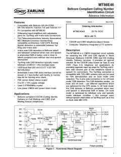
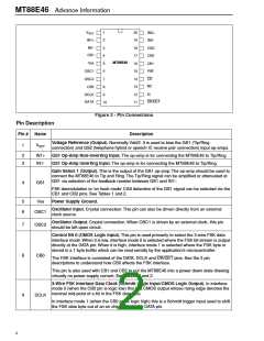
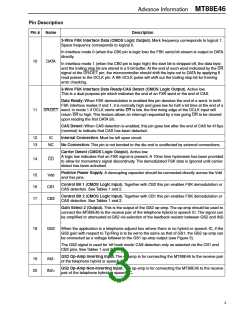
MT88E46 Advance Information
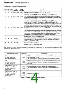
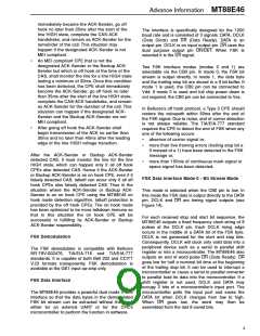
Control Bit (CB0/1/2) Functionality
FSK
Input
CB0 CB1 CB2
Function
Interface Op-Amp
0/1
0/1
1
1
1
0
Set by CB0 GS1 FSK Demodulation. DR/DET pin is the DR signal.
‘Off hook mode’ CAS Detection. DR/DET pin is the DET signal.
The off hook mode algorithm is Bellcore talkoff and talkdown compliant
Set by CB0 GS2
when near end speech level is attenuated 8dB or better. It should be used
for the off hook state CPE.
‘On hook mode’ CAS Detection. DR/DET pin is the DET signal.
When the line is in use, a TIA Multiple Extension Interworking (MEI)
compatible Type 2 CPE must be able to detect CAS even though the CPE
itself is on hook. Since in most telephone designs the hybrid or speech IC
is not operational when the CPE itself is on hook, this mode provides Tip
Set by CB0 GS1 Ring CAS detection for the on hook state MEI CPE.
0/1
0
1
The on hook mode algorithm is optimized for talkdown only and typically
meets talkdown condition 1 (the average case) without near end speech
attenuation. It must not be used when the CPE itself is off hook. See ‘On
Hook Mode CAS Detection’ section in ‘Functional Description’.
Power Down. DR/DET pin is logic high.
The MT88E46 is disabled and draws virtually no power supply current.
Note that the DCLK pin becomes an input pin because FSK interface
mode 1 is selected by CB0=1.
1
0
0
0
0
0
Mode 1
Mode 0
-
-
Reserved for factory testing.
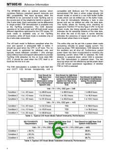
Table 1. CB0/1/2 Function Table
The number of control bits (CB) required to interface the MT88E46 to the microcontroller depends on the
functionality of the application.
Functionality Group
FSK,
Off Hook mode CAS
(Non MEI compatible)
Controls
Description
CB0 is connected to Vdd or Vss to select the FSK interface mode.
CB1 connected to Vdd.
The microcontroller uses CB2 to select between the 2 functions.
CB2
FSK,
CB0 is connected to Vdd or Vss to select the FSK interface mode.
The microcontroller uses CB1 and CB2 to select between the 3
functions.
CB1
CB2
Off Hook mode CAS,
On Hook mode CAS
FSK (Interface mode 1),
Off Hook mode CAS,
On Hook mode CAS,
Power Down
CB0 is connected to Vdd to select FSK interface mode 1.
The microcontroller uses CB1 and CB2 to select between the 4
functions.
CB1
CB2
FSK (Interface mode 0),
Off Hook mode CAS,
On Hook mode CAS,
Power Down
CB0
CB1
CB2
All 3 pins are required.
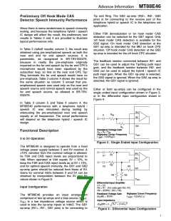
Table 2. Control Bit Functionality Groups
4

 ZARLINK [ ZARLINK SEMICONDUCTOR INC ]