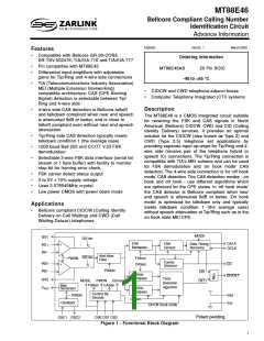
MT88E46 Advance Information
V
1
2
3
4
5
6
7
8
9
10
20
19
18
17
16
15
14
13
12
11
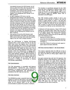
IN2+
IN2-
GS2
CB2
REF
IN1+
IN1-
GS1
MT88E46
Vss
OSC1
OSC2
CB0
CB1
Vdd
CD
NC
IC
DCLK
DATA
DR/DET
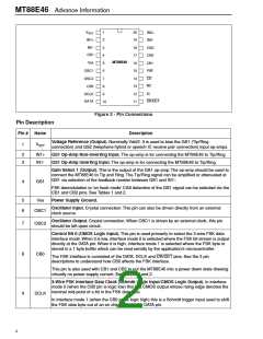
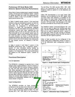
Figure 2 - Pin Connections
Pin Description
Pin # Name
Description
Voltage Reference (Output). Nominally Vdd/2. It is used to bias the GS1 (Tip/Ring
connection) and GS2 (telephone hybrid or speech IC receive pair connection) input op-amps.
1
VREF
2
3
IN1+
IN1-
GS1 Op-Amp Non-inverting Input. The op-amp is for connecting the MT88E46 to Tip/Ring.
GS1 Op-Amp Inverting Input. The op-amp is for connecting the MT88E46 to Tip/Ring.
Gain Select 1 (Output). This is the output of the GS1 op-amp. The op-amp should be used to
connect the MT88E46 to Tip and Ring. The Tip/Ring signal can be amplified or attenuated at
GS1 via selection of the feedback resistor between GS1 and IN1-.
4
GS1
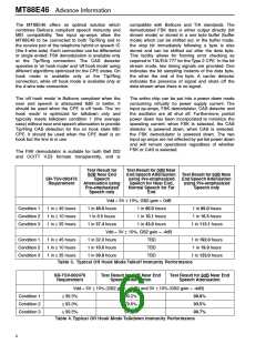
FSK demodulation or ‘on hook mode’ CAS detection of the GS1 signal can be selected via the
CB1 and CB2 pins. See Tables 1 and 2.
5
6
Vss
Power Supply Ground.
Oscillator Input. Crystal connection. This pin can also be driven directly from an external
clock source.
OSC1
Oscillator Output. Crystal connection. When OSC1 is driven by an external clock, this pin
should be left open circuit.
7
OSC2
CB0
Control Bit 0 (CMOS Logic Input). This pin is used primarily to select the 3-wire FSK data
interface mode. When it is low, interface mode 0 is selected where the FSK bit stream is output
directly at the DATA pin. When it is high, interface mode 1 is selected where the FSK byte is
stored in a 1 byte buffer which can be read serially by the application’s microcontroller.
8
The FSK interface is consisted of the DATA, DCLK and DR/DET pins. See the 3 pin
descriptions to understand how CB0 affects the FSK interface.
This pin is also used with CB1 and CB2 to put the MT88E46 into a power down state drawing
virtually no power supply current. See Tables 1 and 2.
3-Wire FSK Interface Data Clock (Schmitt Logic Input/CMOS Logic Output). In interface
mode 0 (when the CB0 pin is logic low) this is a CMOS output whose rising edge denotes the
nominal mid-point of a bit in the FSK data byte.
9
DCLK
In interface mode 1 (when the CB0 pin is logic high) this is a Schmitt trigger input used to shift
the FSK data byte out of an on chip buffer to the DATA pin.
2

 ZARLINK [ ZARLINK SEMICONDUCTOR INC ]