L9216B/H
Preliminary Data Sheet
September 2001
High-Voltage Ringing SLIC with Ground Start
Using REQ, calculate the desired transmit gain, taking
into account the impedance transformation:
600
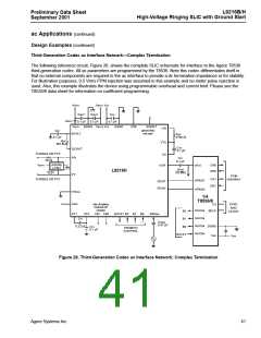
ac Applications (continued)
Design Examples (continued)
TX (dB) = TX (specified[dB]) + 20log
----------
REQ
ac Interface Using First-Generation Codec (contin-
ued)
TX (specified[dB]) is the specified transmit gain. 600 Ω is
the impedance at the PCM, and REQ is the impedance
at
Transmit Gain
600
tip and ring. 20log
represents the power
----------
REQ
Transmit gain will be specified as a gain from T/R to
PCM, TX (dB). Since PCM is referenced to 600 Ω and
assumed to be 0 dB, and in the case of T/R being refer-
enced to some complex impedance other than 600 Ω
resistive, the effects of the impedance transformation
must be taken into account.
loss/gain due to the impedance transformation.
Note that in the case of a 600 Ω pure resistive termina-
tion
600
REQ
600
= 0.
---------
at T/R 20log
= 20log
----------
Again, specified complex termination impedance at T/R
is of the form:
600
Thus, there is no power loss/gain due to impedance
transformation and TX (dB) = TX (specified[dB]).
R2
Finally, convert TX (dB) to a ratio, gTX:
TX (dB) = 20log gTX
R1
C
The ratio of RX/RT6 is used to set the transmit gain:
5-6396(F)
RX
RT6
318.25
20
1
M
First, calculate the equivalent resistance of this network
at the midband frequency of 1000 Hz.
----------
= gTX • ----------------- • ---- with a quad Agere codec
such as T7504:
REQ =
2
2
2
2
2
(2 πf) C1 R1R22 + R1 + R2
2 πfR2 C1
RX < 200 kΩ
-----------------------------------------------------------------------------
--------------------------------------------------
+
2
2
2
2
2
2
1 + (2 πf) R2 C1
1 + (2 πf) R2 C1
RTGS CGS
Rx
RGX = 4750 Ω
–IT/R
0.1 µF
318.25
RT6
–
20
+
VTX
TXI
VITR
CODEC
OP AMP
CN
RT3
RHB
RN1
RN2
RCVN
RCVP
CODEC
OUTPUT
DRIVE
AMP
RRCV
RGP
5-6400.P (F)
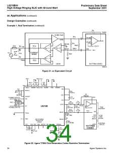
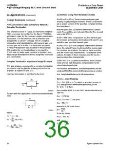
Figure 23. Interface Circuit Using First-Generation Codec (Blocking Capacitors Not Shown)
Agere Systems Inc.
37

 ZARLINK [ ZARLINK SEMICONDUCTOR INC ]