L9216B/H
Preliminary Data Sheet
September 2001
High-Voltage Ringing SLIC with Ground Start
ac Interface Using First-Generation Codec
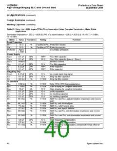
ac Applications (continued)
Design Examples (continued)
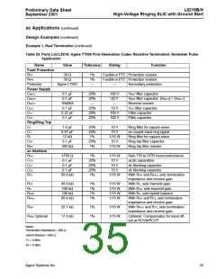
RGX/RTGS/CGS (ZTG): These components give gain
shaping to get good gain flatness. These components
are a scaled version of the specified complex termina-
tion impedance.
First-Generation Codec ac Interface Network—
Complex Termination
Note for pure (600 Ω) resistive terminations, compo-
nents RTGS and CGS are not used. Resistor RGX is used
and is still 4750 Ω.
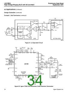
The reference circuit in Figure 25 shows the complete
SLIC schematic for interface to the Agere T7504 first-
generation codec for the German complex termination
impedance. For this example, the ac interface was
designed for a 220 Ω + (820 Ω || 115 nF) complex
termination and hybrid balance with transmit gain and
receive gain set to 0 dBm. For illustration purposes,
1 Vrms PPM injection was assumed in this example.
This implies the overhead voltage is increased to
7.24 V and no meter pulse rejection is required. Also,
this example illustrates the device using fixed overhead
and current limit.
RX/RT6: With other components set, the transmit gain
(for complex and resistive terminations) RX and RT6 are
varied to give specified transmit gain.
RT3/RRCV/RGP: For both complex and resistive termina-
tions, the ratio of these resistors sets the receive gain.
For resistive terminations, the ratio of these resistors
sets the return loss characteristic. For complex termi-
nations, the ratio of these resistors sets the low-fre-
quency return loss characteristic.
CN/RN1/RN2: For complex terminations, these compo-
nents provide high-frequency compensation to the
return loss characteristic.
Complex Termination Impedance Design Example
The gain shaping necessary for a complex termination
impedance may be done by shaping across the AX
amplifier at nodes ITR and VTX.
For resistive terminations, these components are not
used and RCVN is connected to ground via a resistor.
Complex termination is specified in the form:
RHB: Sets hybrid balance for all terminations.
Set ZTG—Gain Shaping:
R2
ZTG = RGX || RTGS + CGS which is a scaled version of
ZT/R (the specified termination resistance) in the
R1´ || R2´ + C´ form.
R1
C
RGX must be 4750 Ω to set SLIC transconductance to
5-6396(F)
300 V/A.
To work with this application, convert termination to the
form:
RGX = 4750 Ω
R1´
At dc, CGS and C´ are open.
RGX = M x R1´
where M is the scale factor.
4750
R2´ C´
--------------
M =
5-6398(F)
R1′
where:
It can be shown:
R1´ = R1 + R2
R1
RTGS = M x R2´
-------
R2´ =
(R1 + R2)
and
R2
C′
M
------
CTGS =
C´ =
2 C
R2
R1 + R2
---------------------
36
Agere Systems Inc.

 ZARLINK [ ZARLINK SEMICONDUCTOR INC ]