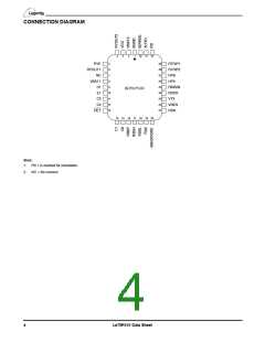
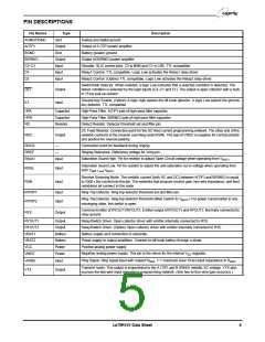
PIN DESCRIPTIONS
Pin Names
AGND/DGND
A(TIP)
Type
Description
Gnd
Analog and digital ground
Output
Gnd
Output of A (TIP) power amplifier
Battery (power) ground
BGND
B(RING)
C3–C1
Output
Input
Input
Input
Output of B(RING) power amplifier
Decoder. SLIC control pins. C3 is MSB and C1 is LSB. TTL compatible.
Relay1 Control. TTL compatible. Logic Low activates the Relay1 relay driver.
Relay2 Control. (Option) TTL compatible. Logic Low activates the Relay2 relay driver.
D1
D2
Switchhook Detector. When enabled, a logic Low indicates that a selected condition is detected. The
detect condition is selected by the logic inputs (C3–C1 and E1). The output is open collector with a built-
in 15 kΩ pull-up resistor.
DET
Output
Ground-Key Enable. (Option) A logic High selects the off-hook detector. A logic Low selects the ground-
key detector. TTL compatible.
E1
Input
HPA
HPB
RD
Capacitor
Capacitor
Resistor
High-Pass Filter. A(TIP) side of high-pass filter capacitor.
High-Pass Filter. B(RING) side of high-pass filter capacitor.
Detect Resistor. Detector threshold set and filter pin.
DC Feed Resistor. Connection point for the DC-feed current programming network. The other end of the
network connects to the receiver summing node (RSN). The sign of VRDC is negative for normal polarity
and positive for reverse polarity.
RDC
Output
RDCR
RREF
RSGH
—
Connection point for feedback during ringing.
—
Ringing Reference. Reference voltage for Vring pin.
Saturation Guard High. Pin for resistor to adjust Open Circuit voltage when operating from V
.
Input
BAT1
Saturation Guard Low. Pin for resistor to adjust the anti-saturation cut-in voltage when operating from
both V
RSGL
RSN
Input
Input
V
.
BAT1 and BAT2
Receive Summing Node. The metallic current (both AC and DC) between A(TIP) and B(RING) is equal
to 1000 x the current into this pin. The networks that program receive gain, two-wire impedance, and feed
resistance all connect to this node.
RTRIP1
RTRIP2
Input
Input
Ring-Trip Detector. Ring-trip detector threshold set and filter pin.
Ring-Trip Detector. Ring-trip detector threshold offset (switch to V
nonringing state, this switch is open.
). For power conservation in any
BAT1
Common Emitter of RYOUT1/RYOUT2. Emitter output of RYOUT1 and RYOUT2. Normally connected to
relay ground.
RYE
Output
RYOUT1
RYOUT2
VBAT1
VBAT2
VCC
Output
Output
Battery
Battery
Power
Power
Relay/Switch Driver. Open collector driver with emitter internally connected to RYE.
Relay/Switch Driver. (Option) Open collector driver with emitter internally connected to RYE.
Battery supply and connection to substrate.
Power supply to output amplifiers. Connect to off-hook battery through a diode.
Positive analog power supply
Negative analog power supply. This pin is the return for the internal V regulator.
VNEG
EE
Ring Signal. Ring signal input with respect R
. 1 V maximum level 10 kΩ input impedance to R
.
REF
VRING
VTX
Input
REF
Transmit Audio. This output is proportional to the A (TIP) and B (RING) metallic AC voltage. VTX also
sources the two-wire input impedance programming network. (See two-to-four-wire gain accuracy.)
Output
Le79R101 Data Sheet
5

 ZARLINK [ ZARLINK SEMICONDUCTOR INC ]