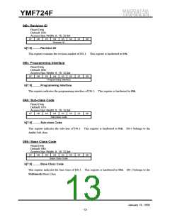
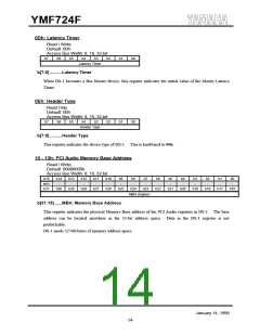
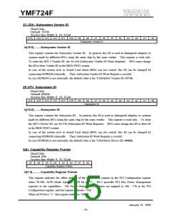
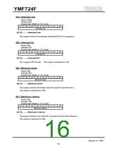
YMF724F
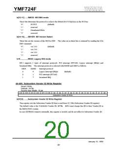
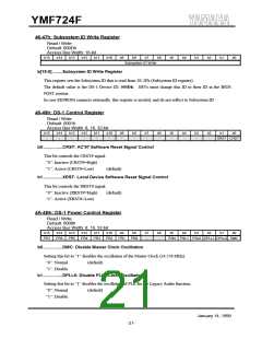
40 - 41h: Legacy Audio Control
Read / Write
Default: 907Fh
Access Bus Width: 8, 16, 32-bit
b15
b14
b13
b12
b11
b10
b9
b8
b7
b6
b5
b4
b3
b2
b1
b0
LAD SIEN
MPUIRQ
SBIRQ
SDMA
I/O
MIEN MEN GPEN FMEN SBEN
b0................SBEN: Sound Blaster Enable
This bit enables the mapping of the Sound Blaster Pro block in the I/O space specified by the SBIO bits,
when LAD is set to “0”. The FM Synthesizer registers can be accessed via SB I/O space, while the SB
block is enabled, even if FMEN is set to “0”.
“0”: Disable the mapping of the SB block to the I/O space
“1”: Enable the mapping of the SB block to the I/O space
(default)
b1................FMEN: FM Synthesizer Enable
This bit enables the mapping of the FM Synthesizer block in the I/O space specified by the FMIO bits,
when LAD is set to “0”. FM Synthesizer registers can be accessed via SB I/O space, while the SB block
is enabled, even if FMEN is set to “0”.
“0”: Disable the mapping of the FM Synthesizer block to the FMIO space
“1”: Enable the mapping of the FM Synthesizer block to the FMIO space
(default)
After setting FMEN to “1”, about 100 msec is necessary before accessing these I/O space.
b2................GPEN: Gameport Enable
This bit enables the mapping of the Joystick block in the I/O space specified by the JSIO bits, when LAD
is set to “0”.
“0”: Disable the mapping of the Joystick block
“1”: Enable the mapping of the Joystick block
(default)
b3................MEN: MPU401 Enable
This bit enables the mapping of the MPU401 block in the I/O space specified by the MPUIO bits, when
LAD is set to “0”.
“0”: Disable the mapping of the MPU401 block
“1”: Enable the mapping of the MPU401 block
(default)
b4................MIEN: MPU401 IRQ Enable
This bit enables the interrupt service of MPU401, when LAD is set to “0” and MEN is set to “1”.
MPU401 generates an interrupt signal when it receives any kind of MIDI data from the RXD pin.
“0”: The MPU401 block can not use the interrupt service.
“1”: The MPU401 block can use interrupt signals determined by the MPUIRQ bits.
(default)
b5................I/O: I/O Address Aliasing Control
This bit selects the number of bits to decode for the I/O address of each block.
“0”: 16-bit address decode
“1”: 10-bit address decode
(default)
January 14, 1999
-17-

 YAMAHA [ YAMAHA CORPORATION ]