R
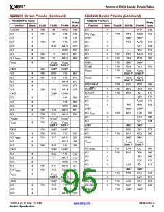
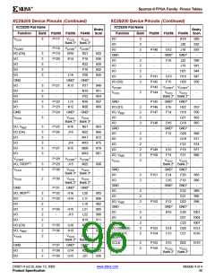
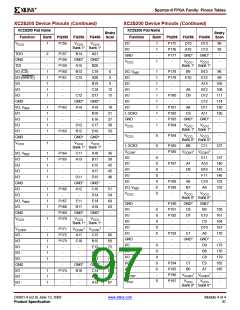
Spartan-II FPGA Family: Pinout Tables
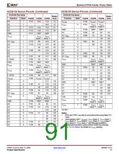
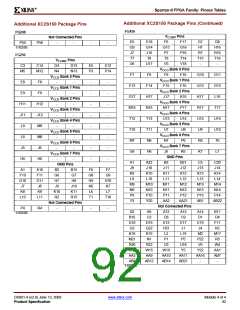
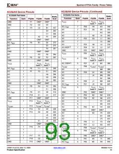
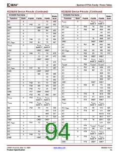
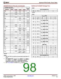
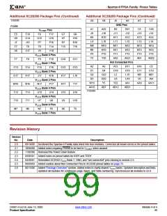
Additional XC2S200 Package Pins (Continued)
Additional XC2S200 Package Pins (Continued)
11/02/00
G6
H6
J6
K6
K7
L7
GND Pins
FG456
A1
J9
A22
J10
B2
B21
J12
C3
J13
K13
L13
M13
N13
P13
AB1
C20
J14
VCCINT Pins
J11
K11
L11
M11
N11
P11
AA2
E5
G9
J7
E18
G14
J16
T8
F6
G15
P7
F17
G16
P16
T14
V18
G7
H7
R7
T15
-
G8
H16
R16
T16
-
K9
L9
M9
N9
P9
Y3
K10
L10
M10
N10
P10
Y20
K12
L12
K14
L14
M12
N12
P12
AA21
M14
N14
P14
AB22
T7
U6
T9
U17
V5
V
V
V
V
V
V
V
V
CCO Bank 0 Pins
F9 F10
CCO Bank 1 Pins
F15 F16
CCO Bank 2 Pins
J17 K16
CCO Bank 3 Pins
N17 P17
CCO Bank 4 Pins
U13 U14
CCO Bank 5 Pins
U7 U8
CCO Bank 6 Pins
N7 P6
CCO Bank 7 Pins
F7
F13
G17
M16
T12
T10
M7
F8
G10
G12
K17
R17
U15
U9
G11
G13
L16
T17
U16
U10
T6
Not Connected Pins
A2
D1
A6
D4
A12
D18
L2
B11
D19
L19
B16
E17
M2
V6
C2
E19
M21
W4
AA11
-
F14
H17
N16
T13
T11
N6
G2
G22
R20
Y5
R3
U3
U18
AA1
AB21
W19
Y22
AB12
AA3
-
AA16
AB7
11/02/00
R6
Revision History
Version
No.
2.0
2.1
2.2
2.3
2.4
2.5
2.8
Date
Description
09/18/00 Sectioned the Spartan-II Family data sheet into four modules. Corrected all known errors in the pinout tables.
10/04/00 Added notes requiring PWDN to be tied to VCCINT when unused.
11/02/00 Removed the Power Down feature.
03/05/01 Added notes on pinout tables for IRDY and TRDY.
04/30/01 Reinstated XC2S50 VCCO Bank 7, GND, and "not connected" pins missing in version 2.3.
09/03/03 Added caution about Not Connected Pins to XC2S30 pinout tables on page 76.
06/13/08 Added "Package Overview" section. Added notes to clarify shared VCCO banks. Updated description and links.
Updated all modules for continuous page, figure, and table numbering. Synchronized all modules to v2.8.
DS001-4 (v2.8) June 13, 2008
Product Specification
www.xilinx.com
Module 4 of 4
99

 XILINX [ XILINX, INC ]