R
Spartan-II FPGA Family: Pinout Tables
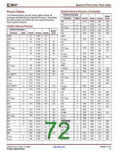
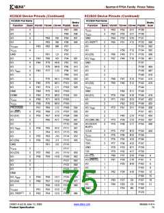
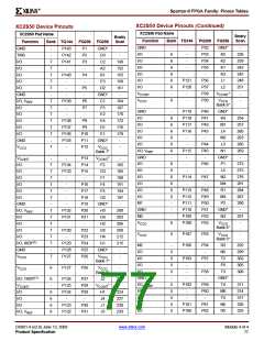
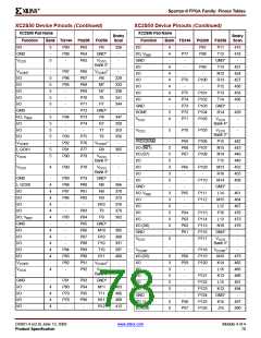
XC2S30 Device Pinouts (Continued)
XC2S30 Device Pinouts (Continued)
XC2S30 Pad Name
XC2S30 Pad Name
Bndry
Bndry
Bank VQ100 TQ144 CS144 PQ208 Scan
Function
VCCINT
Bank VQ100 TQ144 CS144 PQ208 Scan
Function
I/O, VREF
I/O
-
P85
P24
P23
P22
-
A9
D8
C8
-
P171
P172
P173
P174
P175
P176
P177
P178
P179
P180
P181
P182
P183
P184
P184
P185
P186
P187
P188
P189
P190
P191
P192
P193
P194
P195
P196
P197
P198
P199
P200
P201
-
0
0
0
0
-
P97
-
P5
-
C4
-
P203
P204
P205
P206
P207
P208
P208
95
98
101
104
-
I/O
1
1
1
1
1
-
-
24
27
30
33
36
-
I/O
-
I/O
-
P4
P3
P2
P1
P144
A3
B3
C3
A2
B2
I/O
-
I/O
P98
P99
P100
P100
I/O
-
-
-
TCK
I/O
-
-
-
VCCO
0
7
-
GND
I/O, VREF
I/O
-
-
-
VCCO
-
04/18/01
1
1
1
1
1
-
P86
P21
-
B8
-
39
42
45
48
54
-
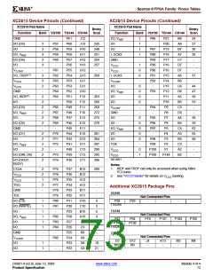
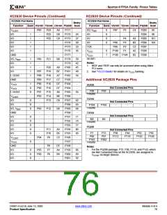
Notes:
-
1. IRDY and TRDY can only be accessed when using Xilinx
PCI cores.
2. See "VCCO Banks" for details on VCCO banking.
I/O
-
P20
P19
P18
P17
P16
P16
P15
P14
P13
-
A8
B7
A7
C7
D7
D7
A6
B6
C6
-
I/O
P87
I, GCK2
GND
VCCO
VCCO
I, GCK3
VCCINT
I/O
P88
P89
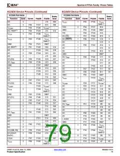
Additional XC2S30 Package Pins
1
0
0
-
P90
-
VQ100
Not Connected Pins
P90
-
P28
11/02/00
P29
P105
N3
-
-
-
-
-
-
-
-
P91
55
-
P92
TQ144
0
0
0
-
-
62
65
68
-
Not Connected Pins
I/O
-
P104
11/02/00
-
-
I/O, VREF
GND
I/O
P93
P12
-
D6
-
-
CS144
Not Connected Pins
0
0
0
0
0
-
-
-
-
71
74
77
80
83
-
M3
-
-
I/O
-
-
-
11/02/00
I/O
-
-
-
PQ208
I/O
-
P11
P10
P9
-
A5
B5
C5
-
Not Connected Pins
P7
P60
P13
P97
P38
P112
-
P44
P118
-
P55
P143
-
P56
P149
-
I/O
-
P94
-
VCCINT
VCCO
GND
I/O
P165
P202
0
-
-
11/02/00
-
P8
P7
P6
-
D5
A4
B4
-
-
Notes:
1. For the PQ208 package, P13, P38, P118, and P143, which
are Not Connected Pins on the XC2S30, are assigned to
VCCINT on larger devices.
0
0
0
P95
P96
-
86
89
92
I/O
I/O
DS001-4 (v2.8) June 13, 2008
Product Specification
www.xilinx.com
Module 4 of 4
76

 XILINX [ XILINX, INC ]