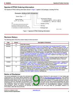
Spartan-6 Family Overview
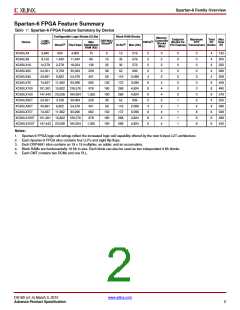
Spartan-6 FPGA Device-Package Combinations and Available I/Os
Spartan-6 FPGA package combinations with the available I/Os and GTP transceivers per package are shown in Table 2.
Due to the transceivers, the LX and LXT pinouts are not compatible.
Table 2: Spartan-6 Device-Package Combinations and Maximum Available I/Os
Package
Size (mm)
Pitch (mm)
CPG196(1) TQG144(1) CSG225(2) FT(G)256(3)
CSG324
15 x 15
0.8
FG(G)484(3,4)
23 x 23
1.0
CSG484(4)
19 x 19
0.8
FG(G)676(3)
27 x 27
1.0
FG(G)900(3)
31 x 31
1.0
8 x 8
0.5
20 x 20
0.5
13 x 13
0.8
17 x 17
1.0
User
I/O
User
GTPs
User
GTPs
User
GTPs
User
GTPs
Device
User I/O
User I/O
User I/O
User I/O
GTPs
I/O
I/O
I/O
I/O
XC6SLX4
106
106
106
102
102
132
160
160
XC6SLX9
186
186
186
NA
NA
NA
NA
200
232
226
218
XC6SLX16
XC6SLX25
XC6SLX45
XC6SLX75
XC6SLX100
XC6SLX150
XC6SLX25T
XC6SLX45T
XC6SLX75T
XC6SLX100T
XC6SLX150T
NA
NA
NA
NA
NA
2
266
316
280
326
338
250
296
268
296
296
NA
NA
NA
NA
320
328
338
338
NA
NA
NA
NA
358
408
480
498
NA
576
2
4
190
190
4
4
4
4
4
296
292
296
296
4
8
8
8
348
376
396
4
8
8
498
540
4
Notes:
1. There is no memory controller on the devices in these packages.
2. Memory controller block support is x8 on the XC6SLX9 and XC6SLX16 devices in the CSG225 package. There is no memory controller in the
XC6SLX4.
3. These devices are available in both Pb and Pb-free (additional G) packages as standard ordering options.
4. These packages support two of the four memory controllers in the XC6SLX75, XC6SLX75T, XC6SLX100, XC6SLX100T, XC6SLX150, and
XC6SLX150T devices.
Configuration
Spartan-6 FPGAs store the customized configuration data in SRAM-type internal latches. The number of configuration bits
is between 2.6 Mb and 33 Mb depending on device size but independent of the specific user-design implementation, unless
compression mode is used. The configuration storage is volatile and must be reloaded whenever the FPGA is powered up.
This storage can also be reloaded at any time by pulling the PROGRAM_B pin Low. Several methods and data formats for
loading configuration are available.
Bit-serial configurations can be either master serial mode, where the FPGA generates the configuration clock (CCLK) signal,
or slave serial mode, where the external configuration data source also clocks the FPGA. For byte-wide configurations,
master SelectMAP mode generates the CCLK signal while slave SelectMAP mode receives the CCLK signal for the 8- and
16-bit-wide transfer. In master serial mode, the beginning of the bitstream can optionally switch the clocking source to an
external clock, which can be faster or more precise than the internal clock. The available JTAG pins use boundary-scan
protocols to load bit-serial configuration data.
DS160 (v1.4) March 3, 2010
www.xilinx.com
Advance Product Specification
3

 XILINX [ XILINX, INC ]