XC4000E Logic Cell Array Family
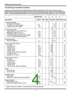
CLB Switching Characteristic Guidelines
Testing of the switching parameters is modeled after testing methods specified by MIL-M-38510/605. All devices are 100%
functionally tested. Since many internal timing parameters cannot be measured directly, they are derived from benchmark timing
patterns. The following guidelines reflect worst-case values over the recommended operating conditions. For more detailed, more
precise, and more up-to-date timing information, use the values provided by the XACT timing calculator and used in the simulator.
Speed Grade
Symbol
-4
-3
-2
Description
Min Max Min Max Min Max Units
Combinatorial Delays
F/G inputs to X/Y outputs
F/G inputs via H’ to X/Y outputs
C inputs via H’ to X/Y outputs
TILO
TIHO
THHO
2.0
3.6
2.9
ns
ns
ns
CLB Fast Carry Logic
Operand inputs (F1,F2,G1,G4) to COUT
Add/Subtract input (F3) to COUT
Initialization inputs (F1,F3) to COUT
CIN through function generators to X/Y outputs
CIN to COUT, bypass function generators.
TOPCY
TASCY
TINCY
TSUM
TBYP
2.6
4.4
1.7
3.3
0.7
ns
ns
ns
ns
ns
Sequential Delays
Clock K to outputs Q
TCKO
2.4
ns
Set-up Time before Clock K
F/G inputs
TICK
2.3
4.0
3.3
1.9
2.6
1.7
ns
ns
ns
ns
ns
ns
ns
ns
F/G inputs via H’
C inputs via H1
C inputs via DIN
C inputs via EC
C inputs via S/R, going Low (inactive)
CIN input via F'/G'
CIN input via F'/G' and H'
TIHCK
THHCK
TDICK
TECCK
TRCK
TCCK
TCHCK
Hold Time after Clock K
F/G inputs
TCKI
0
0
0
0
0
0
ns
ns
ns
ns
ns
ns
F/G inputs via H’
C inputs via H1
C inputs via DIN
C inputs via EC
TCKIH
TCKHH
TCKDI
TCKEC
TCKR
C inputs via S/R, going Low (inactive)
Clock
Clock High time
Clock Low time
TCH
TCL
4.0
4.0
ns
ns
Set/Reset Direct
Width (High)
Delay from C inputs via S/R, going High to Q
TRPW
TRIO
4.0
ns
ns
4.0
Master Set/Reset*
Width (High or Low)
Delay from Global Set/Reset net to Q
TMRW
TMRQ
18.9
ns
ns
14.4
*
Timing is based on the XC4005E. For other devices see XACT timing calculator.
4

 XILINX [ XILINX, INC ]