Spartan-3E FPGA Family: Pinout Descriptions
FT256: 256-ball Fine-pitch, Thin Ball Grid Array
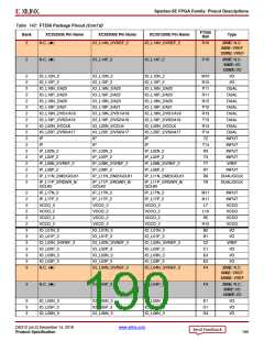
The 256-ball fine-pitch, thin ball grid array package, FT256,
supports three different Spartan-3E FPGAs, including the
XC3S250E, the XC3S500E, and the XC3S1200E.
to a VREF pin on the XC3S500E and XC3S1200E FPGA. If
the FPGA application uses an I/O standard that requires a
VREF voltage reference, connect the highlighted pin to the
VREF voltage supply, even though this does not actually
connect to the XC3S250E FPGA. This VREF connection on
the board allows future migration to the larger devices
without modifying the printed-circuit board.
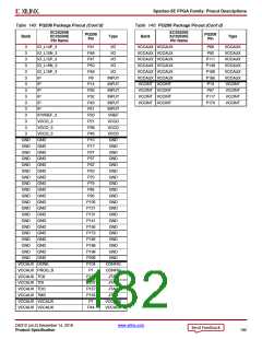
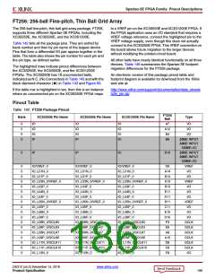
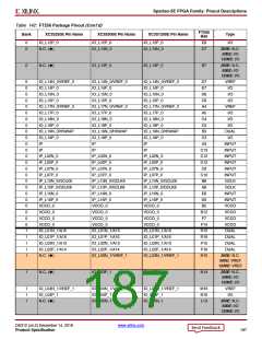
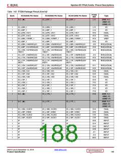
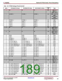
Table 142 lists all the package pins. They are sorted by
bank number and then by pin name of the largest device.
Pins that form a differential I/O pair appear together in the
table. The table also shows the pin number for each pin and
the pin type, as defined earlier.
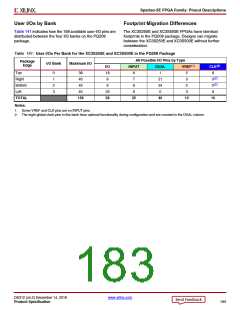
All other balls have nearly identical functionality on all three
devices. Table 146 summarizes the Spartan-3E footprint
migration differences for the FT256 package.
The highlighted rows indicate pinout differences between
the XC3S250E, the XC3S500E, and the XC3S1200E
FPGAs. The XC3S250E has 18 unconnected balls,
indicated as N.C. (No Connection) in Table 142 and with the
black diamond character () in Table 142 and Figure 83.
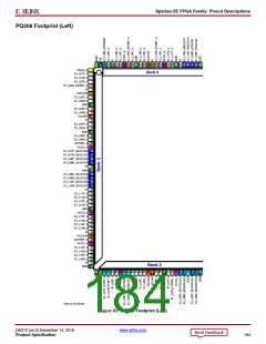
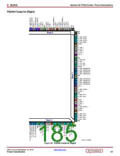
An electronic version of this package pinout table and
footprint diagram is available for download from the Xilinx
web site at:
If the table row is highlighted in tan, then this is an instance
where an unconnected pin on the XC3S250E FPGA maps
http://www.xilinx.com/support/documentation/data_sheets
/s3e_pin.zip
Pinout Table
Table 142: FT256 Package Pinout
FT256
Ball
Bank
XC3S250E Pin Name
XC3S500E Pin Name
XC3S1200E Pin Name
Type
0
0
0
0
IO
IO
IO
IP
IO
IO
IO
IP
IO
IO
IO
IO
A7
I/O
I/O
I/O
A12
B4
B6
250E: INPUT
500E: INPUT
1200E: I/O
0
IP
IP
IO
B10
250E: INPUT
500E: INPUT
1200E: I/O
0
0
0
0
0
0
0
0
0
0
0
0
0
0
0
0
0
0
IO/VREF_0
IO/VREF_0
IO/VREF_0
D9
A14
B14
A13
B13
E11
D11
B11
C11
E10
D10
F9
VREF
I/O
IO_L01N_0
IO_L01N_0
IO_L01N_0
IO_L01P_0
IO_L01P_0
IO_L01P_0
I/O
IO_L03N_0/VREF_0
IO_L03P_0
IO_L03N_0/VREF_0
IO_L03P_0
IO_L03N_0/VREF_0
IO_L03P_0
VREF
I/O
IO_L04N_0
IO_L04N_0
IO_L04N_0
I/O
IO_L04P_0
IO_L04P_0
IO_L04P_0
I/O
IO_L05N_0/VREF_0
IO_L05P_0
IO_L05N_0/VREF_0
IO_L05P_0
IO_L05N_0/VREF_0
IO_L05P_0
VREF
I/O
IO_L06N_0
IO_L06N_0
IO_L06N_0
I/O
IO_L06P_0
IO_L06P_0
IO_L06P_0
I/O
IO_L08N_0/GCLK5
IO_L08P_0/GCLK4
IO_L09N_0/GCLK7
IO_L09P_0/GCLK6
IO_L11N_0/GCLK11
IO_L11P_0/GCLK10
IO_L12N_0
IO_L08N_0/GCLK5
IO_L08P_0/GCLK4
IO_L09N_0/GCLK7
IO_L09P_0/GCLK6
IO_L11N_0/GCLK11
IO_L11P_0/GCLK10
IO_L12N_0
IO_L08N_0/GCLK5
IO_L08P_0/GCLK4
IO_L09N_0/GCLK7
IO_L09P_0/GCLK6
IO_L11N_0/GCLK11
IO_L11P_0/GCLK10
IO_L12N_0
GCLK
GCLK
GCLK
GCLK
GCLK
GCLK
I/O
E9
A9
A10
D8
C8
F8
DS312 (v4.2) December 14, 2018
www.xilinx.com
Product Specification
186

 XILINX [ XILINX, INC ]