Spartan-3E FPGA Family: Pinout Descriptions
User I/Os by Bank
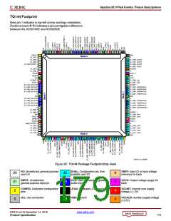
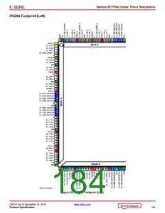
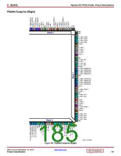
Footprint Migration Differences
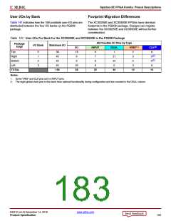
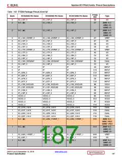
Table 141 indicates how the 158 available user-I/O pins are
distributed between the four I/O banks on the PQ208
package.
The XC3S250E and XC3S500E FPGAs have identical
footprints in the PQ208 package. Designs can migrate
between the XC3S250E and XC3S500E without further
consideration.
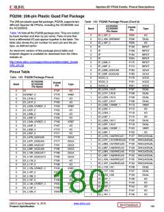
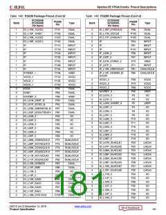
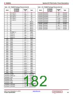
Table 141: User I/Os Per Bank for the XC3S250E and XC3S500E in the PQ208 Package
All Possible I/O Pins by Type
Package
I/O Bank
Maximum I/O
Edge
(2)
I/O
18
9
INPUT
DUAL
VREF(1)
CLK
Top
0
1
2
3
38
40
6
7
1
5
3
8
(2)
Right
21
24
0
0
0
(2)
Bottom
Left
40
8
6
2
40
23
58
6
3
8
TOTAL
158
25
46
13
16
Notes:
1. Some VREF and CLK pins are on INPUT pins.
2. The eight global clock pins in this bank have optional functionality during configuration and are counted in the DUAL column.
DS312 (v4.2) December 14, 2018
www.xilinx.com
Product Specification
183

 XILINX [ XILINX, INC ]