Spartan-6 FPGA Data Sheet: DC and Switching Characteristics
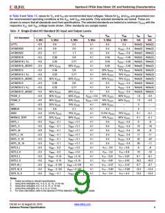
Table 2: Recommended Operating Conditions(1) (Cont’d)
Memory
Temperature Speed
Range Grade
Controller
Symbol
Description
Min
Typ
Max
Units
(2)
Block
Performance
Maximum current through pin using PCI Commercial -4, -3, -2,
N/A
–
–
–
–
10
10
mA
mA
I/O standard when forward biasing the
clamp diode.
-1L(7)
(8)
IIN
Industrial
-3, -2,
-1L(7)
N/A
N/A
Battery voltage relative to GND, Tj = 0°C Commercial -4, -3, -2,
to +85°C
-1L
(XC6SLX75, XC6SLX75T, XC6SLX100,
XC6SLX100T, XC6SLX150, and
XC6SLX150T only)
(9)
VBATT
1.0
–
3.6
V
Battery voltage relative to GND,
Tj = –40°C to +100°C (XC6SLX75,
XC6SLX75T, XC6SLX100,
XC6SLX100T, XC6SLX150, and
XC6SLX150T only)
Industrial
-3, -2, -1L
N/A
Notes:
1. All voltages are relative to ground.
2. See Interface Performances for Memory Interfaces in Table 25. The standard V
voltage range applies to designs not using an MCB, or to devices
CCINT
that do not support MCB functionality including the LX4 device, the TQG144 and CPG196 packages, and the -3N speed grade.
3. Recommended maximum voltage droop for V is 10 mV/ms.
CCAUX
4. Configuration data is retained even if V
drops to 0V.
CCO
5. Includes V
of 1.2V, 1.5V, 1.8V, 2.5V, and 3.3V.
CCO
6. For PCI systems, the transmitter and receiver should have common supplies for V
7. Devices with a -1L speed grade do not support Xilinx PCI IP.
8. Do not exceed a total of 100 mA per bank.
.
CCO
9.
V
is required to maintain the battery backed RAM (BBR) AES key when V
is not applied. Once V
is applied, V can be
BATT
BATT
CCAUX
CCAUX
unconnected. When BBR is not used, Xilinx recommends connecting to V
or GND. However, V
can be unconnected.
CCAUX
BATT
Table 3: eFUSE Programming Conditions(1)
Symbol
Description
Min
3.2
–
Typ
Max Units
(2)
VFS
External voltage supply
VFS supply current
3.3
–
3.4
40
V
mA
V
IFS
VCCAUX Auxiliary supply voltage relative to GND
3.2
3.3
3.45
(3)
RFUSE
External resistor from RFUSE pin to GND
1129 1140 1151
Ω
VCCINT Internal supply voltage relative to GND
1.14
15
1.2
–
1.26
85
V
tj
Temperature range
°C
Notes:
1. These specifications apply during programming of the eFUSE AES key. Programming is only supported through JTAG.The AES key is only supported
in the following devices: XC6SLX75, XC6SLX75T, XC6SLX100, XC6SLX100T, XC6SLX150, and XC6SLX150T.
2. When programming eFUSE, V must be less than or equal to V
. When not programming or when eFUSE is not used, Xilinx recommends
CCAUX
FS
connecting V to GND. However, V can be between GND and 3.45 V.
FS
FS
3. An R
resistor is required when programming the eFUSE AES key. When not programming or when eFUSE is not used, Xilinx recommends
FUSE
connecting the R
pin to V
or GND. However, R
can be unconnected.
FUSE
FUSE
CCAUX
DS162 (v1.9) August 23, 2010
Advance Product Specification
www.xilinx.com
3

 XILINX [ XILINX, INC ]