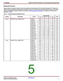
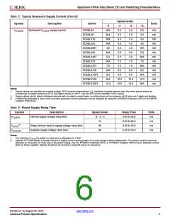
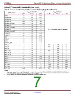
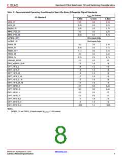
Spartan-6 FPGA Data Sheet: DC and Switching Characteristics
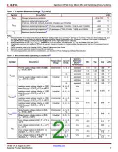
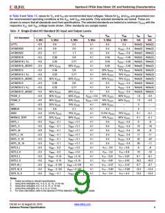
Table 4: DC Characteristics Over Recommended Operating Conditions
Symbol
VDRINT
VDRAUX
IREF
Description
Data retention VCCINT voltage (below which configuration data might be lost)
Data retention VCCAUX voltage (below which configuration data might be lost)
VREF leakage current per pin
Min
0.8
Typ
–
Max Units
–
V
2.0
–
–
V
–10
–10
–20
–
10
10
20
µA
µA
µA
IL
Input or output leakage current per pin (sample-tested)
–
All pins except PROGRAM_B, DONE, and
–
JTAG pins when HSWAPEN = 1
Leakage current on pins during hot
IHS
socketing with FPGA unpowered
PROGRAM_B, DONE, and JTAG pins, or other
IHS + IRPU
µA
pins when HSWAPEN = 0
CIN
Die input capacitance at the pad
–
200
120
60
40
12
200
140
–
–
–
10
500
350
200
150
100
550
400
150
–
pF
µA
µA
µA
µA
µA
µA
µA
nA
Ω
Pad pull-up (when selected) @ VIN = 0V, VCCO = 3.3V or VCCAUX = 3.3V
Pad pull-up (when selected) @ VIN = 0V, VCCO = 2.5V or VCCAUX = 2.5V
Pad pull-up (when selected) @ VIN = 0V, VCCO = 1.8V
Pad pull-up (when selected) @ VIN = 0V, VCCO = 1.5V
Pad pull-up (when selected) @ VIN = 0V, VCCO = 1.2V
Pad pull-down (when selected) @ VIN = VCCO, VCCAUX = 3.3V
Pad pull-down (when selected) @ VIN = VCCO, VCCAUX = 2.5V
Battery supply current
–
IRPU
–
–
–
–
IRPD
–
(1)
IBATT
–
(2)
RDT
Resistance of optional input differential termination circuit, VCCAUX = 3.3V
–
100
25
Thevenin equivalent resistance of programmable input termination
(UNTUNED_SPLIT_25)
23
55
Ω
Thevenin equivalent resistance of programmable input termination
(UNTUNED_SPLIT_50)
39
56
50
75
72
Ω
Ω
(4)
RIN_TERM
Thevenin equivalent resistance of programmable input termination
(UNTUNED_SPLIT_75)
109
Notes:
1. Maximum value specified for worst case process at 25°C. XC6SLX75, XC6SLX75T, XC6SLX100, XC6SLX100T, XC6SLX150, and XC6SLX150T
only.
2. Refer to IBIS models for R variation and for values at V
= 2.5V.
DT
CCAUX
3.
V
is not required for data retention. The minimum V
for power-on reset and configuration is 1.65V.
CCO2
CCO2
4. Termination resistance to a V
/2 level.
CCO
DS162 (v1.9) August 23, 2010
Advance Product Specification
www.xilinx.com
4

 XILINX [ XILINX, INC ]