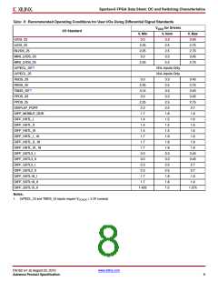
Spartan-6 FPGA Data Sheet: DC and Switching Characteristics
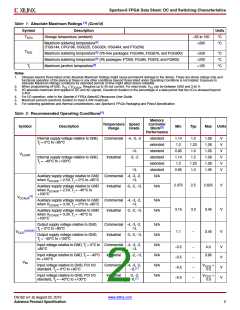
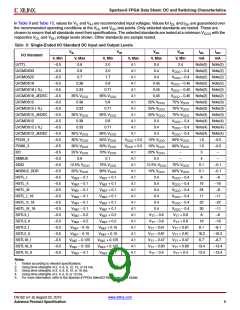
Table 1: Absolute Maximum Ratings (1) (Cont’d)
Symbol
Description
Units
TSTG
Storage temperature (ambient)
–65 to 150
+260
°C
°C
Maximum soldering temperature(6)
(TQG144, CPG196, CSG225, CSG324, CSG484, and FTG256)
TSOL
Maximum soldering temperature(6) (Pb-free packages: FGG484, FGG676, and FGG900)
Maximum soldering temperature(6) (Pb packages: FT256, FG484, FG676, and FG900)
Maximum junction temperature(6)
+250
+220
+125
°C
°C
°C
Tj
Notes:
1. Stresses beyond those listed under Absolute Maximum Ratings might cause permanent damage to the device. These are stress ratings only, and
functional operation of the device at these or any other conditions beyond those listed under Operating Conditions is not implied. Exposure to
Absolute Maximum Ratings conditions for extended periods of time might affect device reliability.
2. When programming eFUSE, V ≤ V
. Requires up to 40 mA current. For read mode, V can be between GND and 3.45 V.
3. I/O absolute maximum limit applied to DC and AC signals. Overshoot duration is the percentage of a data period that the I/O is stressed beyond
FS
CCAUX
FS
3.45V.
4. For I/O operation, refer to the Spartan-6 FPGA SelectIO Resources User Guide.
5. Maximum percent overshoot duration to meet 4.40V maximum.
6. For soldering guidelines and thermal considerations, see Spartan-6 FPGA Packaging and Pinout Specification.
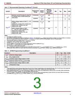
Table 2: Recommended Operating Conditions(1)
Memory
Temperature Speed
Range Grade
Controller
Symbol
Description
Min
Typ
Max
Units
(2)
Block
Performance
standard
extended
standard
standard
extended
standard
N/A
Internal supply voltage relative to GND,
Tj = 0°C to +85°C
Commercial -4, -3, -2
1.14
1.2
1.2
1.23
1.0
1.26
1.26
1.05
1.26
1.26
1.05
V
V
V
V
V
V
-1L
0.95
1.14
1.2
VCCINT
Internal supply voltage relative to GND,
Tj = –40°C to +100°C
Industrial
-3, -2
-1L
1.2
1.23
1.0
0.95
Auxiliary supply voltage relative to GND Commercial -4, -3, -2,
when VCCAUX = 2.5V, Tj = 0°C to +85°C
-1L
2.375
2.5
2.625
V
Auxiliary supply voltage relative to GND
when VCCAUX = 2.5V, Tj = –40°C to
+100°C
Industrial
-3, -2, -1L
N/A
(3)
VCCAUX
Auxiliary supply voltage relative to GND Commercial -4, -3, -2,
N/A
N/A
when VCCAUX = 3.3V, Tj = 0°C to +85°C
-1L
3.15
1.1
3.3
–
3.45
3.45
V
V
Auxiliary supply voltage relative to GND
when VCCAUX = 3.3V, Tj = –40°C to
+100°C
Industrial
-3, -2, -1L
Output supply voltage relative to GND,
Tj = 0°C to +85°C
Commercial -4, -3, -2,
-1L
N/A
N/A
N/A
N/A
N/A
N/A
(4)(5)(6)
VCCO
Output supply voltage relative to GND,
Tj = –40°C to +100°C
Industrial
-3, -2, -1L
Input voltage relative to GND, Tj = 0°C to Commercial -4, -3, -2,
+85°C
–0.5
–0.5
–0.5
–0.5
–
–
–
–
4.0
V
V
V
V
-1L
Input voltage relative to GND, Tj = –40°C
to +100°C
Industrial
-3, -2, -1L
3.95
VIN
Input voltage relative to GND, PCI I/O
standard, Tj = 0°C to +85°C
Commercial -4, -3, -2,
-1L(7)
VCCO
0.5
+
Input voltage relative to GND, PCI I/O
standard, Tj = –40°C to +100°C
Industrial
-3, -2,
-1L(7)
VCCO
0.5
+
DS162 (v1.9) August 23, 2010
www.xilinx.com
Advance Product Specification
2

 XILINX [ XILINX, INC ]