R
Spartan and Spartan-XL FPGA Families Data Sheet
Spartan-XL Family VCC Clamping
Table 4: Supported Sources for Spartan/XL Inputs
Spartan-XL FPGAs have an optional clamping diode con-
nected from each I/O to VCC. When enabled they clamp
ringing transients back to the 3.3V supply rail. This clamping
action is required in 3.3V PCI applications. VCC clamping is
a global option affecting all I/O pins.
Spartan
Inputs
Spartan-XL
Inputs
3.3V
5V,
5V,
Source
TTL CMOS
CMOS
Spartan-XL devices are fully 5V TTL I/O compatible if VCC
clamping is not enabled. With VCC clamping enabled, the
Spartan-XL devices will begin to clamp input voltages to
one diode voltage drop above VCC. If enabled, TTL I/O com-
patibility is maintained but full 5V I/O tolerance is sacrificed.
The user may select either 5V tolerance (default) or 3.3V
PCI compatibility. In both cases negative voltage is clamped
to one diode voltage drop below ground.
Any device, VCC = 3.3V,
CMOS outputs
√
√
√
√
Unreli-
able
Data
√
√
√
Spartan family, VCC = 5V,
TTL outputs
Any device, VCC = 5V,
TTL outputs (VOH ≤ 3.7V)
Any device, VCC = 5V,
CMOS outputs
√
√ (default
mode)
Spartan-XL devices are compatible with TTL, LVTTL, PCI
3V, PCI 5V and LVCMOS signalling. The various standards
are illustrated in Table 5.
Table 5: I/O Standards Supported by Spartan-XL FPGAs
Signaling
Standard
VCC
Clamping
Output
Drive
VIH MAX
5.5
VIH MIN
2.0
VIL MAX
0.8
VOH MIN
2.4
VOL MAX
0.4
TTL
LVTTL
Not allowed
OK
12/24 mA
12/24 mA
24 mA
3.6
2.0
0.8
2.4
0.4
PCI5V
Not allowed
Required
OK
5.5
2.0
0.8
2.4
0.4
PCI3V
12 mA
3.6
50% of VCC
50% of VCC
30% of VCC
30% of VCC
90% of VCC
90% of VCC
10% of VCC
10% of VCC
LVCMOS 3V
12/24 mA
3.6
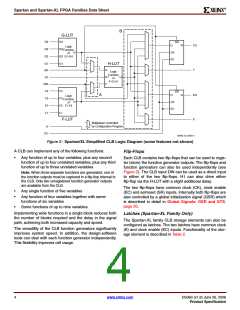
Additional Fast Capture Input Latch (Spartan-XL Family
Only)
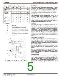
Table 6: Output Flip-Flop Functionality
Clock
The Spartan-XL family OB has an additional optional latch
on the input. This latch is clocked by the clock used for the
output flip-flop rather than the input clock. Therefore, two
different clocks can be used to clock the two input storage
elements. This additional latch allows the fast capture of
input data, which is then synchronized to the internal clock
by the IOB flip-flop or latch.
Mode
Clock Enable
T
D
Q
Power-Up
or GSR
X
X
0*
X
SR
Flip-Flop
X
0
1*
X
0*
0*
1
X
D
X
X
Q
D
Z
X
0
To place the Fast Capture latch in a design, use one of the
special library symbols, ILFFX or ILFLX. ILFFX is a trans-
parent-Low Fast Capture latch followed by an active High
input flip-flop. ILFLX is a transparent Low Fast Capture latch
followed by a transparent High input latch. Any of the clock
inputs can be inverted before driving the library element,
and the inverter is absorbed into the IOB.
X
0*
Q
Legend:
X
Don’t care
Rising edge (clock not inverted).
SR
0*
1*
Z
Set or Reset value. Reset is default.
IOB Output Signal Path
Input is Low or unconnected (default value)
Input is High or unconnected (default value)
3-state
Output signals can be optionally inverted within the IOB,
and can pass directly to the output buffer or be stored in an
edge-triggered flip-flop and then to the output buffer. The
functionality of this flip-flop is shown in Table 6.
8
www.xilinx.com
DS060 (v1.8) June 26, 2008
Product Specification

 XILINX [ XILINX, INC ]