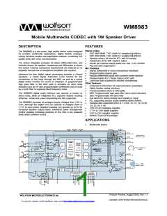
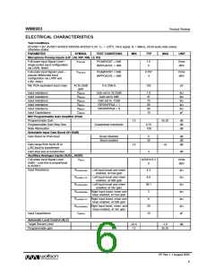
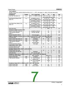
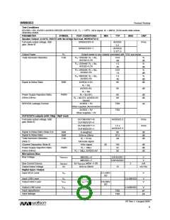
WM8983
Product Preview
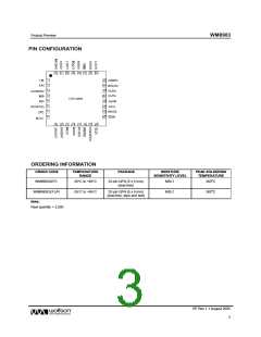
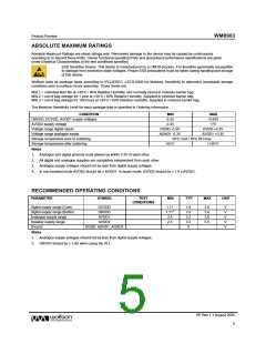
PIN DESCRIPTION
PIN
1
NAME
LIP
TYPE
Analogue input
Analogue input
Analogue input
Analogue input
Analogue input
Analogue input
Digital Input / Output
Digital Input / Output
Digital Output
Digital Input
DESCRIPTION
Left MIC pre-amp positive input
Left MIC pre-amp negative input
2
LIN
3
L2/GPIO2
RIP
Left channel line input/secondary mic pre-amp positive input/GPIO2 pin
Right MIC pre-amp positive input
4
5
RIN
Right MIC pre-amp negative input
6
R2/GPIO3
LRC
Right channel line input/secondary mic pre-amp positive input/GPIO3 pin
DAC and ADC sample rate clock
7
8
BCLK
Digital audio bit clock
9
ADCDAT
DACDAT
MCLK
ADC digital audio data output
10
11
12
13
14
15
16
17
18
19
20
21
22
23
24
25
26
27
28
DAC digital audio data input
Digital Input
Master clock input
DGND
DCVDD
DBVDD
CSB/GPIO1
SCLK
Supply
Digital ground
Supply
Digital core logic supply
Supply
Digital buffer (I/O) supply
Digital Input / Output
Digital Input
3-Wire control interface chip Select / GPIO1 pin
3-Wire control interface clock input / 2-wire control interface clock input
3-Wire control interface data input / 2-Wire control interface data input
Control interface selection
SDIN
Digital Input / Output
Digital Input
MODE
AUXL
Analogue input
Analogue input
Analogue Output
Analogue Output
Analogue Output
Supply
Left auxillary input
AUXR
Right auxillary input
OUT4
right line output or mono mix output
mono or left line output
OUT3
ROUT2
AGND2
LOUT2
AVDD2
VMID
Headphone or line output right 2
Analogue ground (feeds ROUT2/LOUT2 and OUT3/OUT4)
Headphone or line output left 2
Analogue Output
Supply
Analogue supply (feeds output amplifiers ROUT2/LOUT2 and OUT3/OUT4)
Decoupling for ADC and DAC reference voltage
Reference
AGND1
Supply
Analogue ground (feeds all input amplifiers, PLL, ADC and DAC, internal
bias circuits, output amplifiers LOUT1, ROUT1)
29
30
31
ROUT1
LOUT1
AVDD1
Analogue Output
Analogue Output
Supply
Headphone or line output right 1
Headphone or line output left 1
Analogue supply (feeds all input amplifiers, PLL, ADC and DAC, internal
bias circuits, output amplifiers LOUT1, LOUT2))
32
MICBIAS
Analogue Output
Microphone bias
Note:
It is recommended that the QFN ground paddle should be connected to analogue ground on the application PCB.
PP Rev 1.1 August 2005
w
4

 WOLFSON [ WOLFSON MICROELECTRONICS PLC ]