WM8805
Production Data
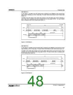
NON-AUDIO DETECTION
The SPDIF payload can contain PCM data for audio or non-audio applications. In the case where the
payload contains the 96 bit synchronization code defined in IEC61937 then this indicates that the
payload contains data which is not suitable for direct playback through an audio codec. This 96 bit
code is defined as 4*16bits of ‘0’+Pa (16bits)+Pb (16bits)..
If the S/PDIFRx interface decodes this sync code then it sets the PCM_N bit.
When the PCM_N =1, then it indicates non-audio data. When the PCM_N =0, then it indicates that
the SPDIF payload does not contain the synch code..
Another status bit, AUDIO_N status is recovered from the Channel Status block. It is bit 1 of the
channel status. When AUDIO_N =0, then it indicates that the SPDIF payload contains audio PCM
encoded data. This is also referred to as linear PCM data. When the AUDIO_N= 1, then it indicates
that the SPDIF payload does not contain audio PCM data.
NON_AUDIO data is indicated by a logical OR of the AUDIO_N and PCM_N flags.
Any change of AUDIO_N or PCM_N status will cause an INT_N interrupt (UPD_NON_AUDIO) to be
generated. If the MASK register bit for AUDIO_N or PCM_N is set, then the associated signal will not
generate an interrupt (UPD_NON_AUDIO).
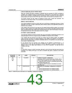
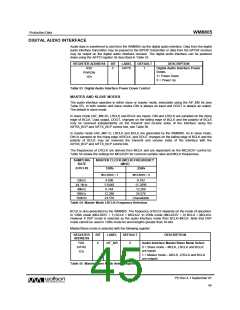
GENERAL PURPOSE OUTPUT (GPO) CONFIGURATION
The WM8805 has a maximum of eight configurable GPO pins depending upon the mode of operation
of the device. By default GPO0 and GPO1 are available, however if 2-wire Software Control Mode is
selected the CSB pin becomes GPO2 and the SDOUT pin becomes GPO7. Finally, if SPDGPO is
set high, pins RX4-RX7 become GPO3-GPO6 respectively.
REGISTER
ADDRESS
BIT
LABEL
DEFAULT
DESCRIPTION
R23
GPO01
17h
3:0
GPO0[3:0]
0000
Flags and Status bits available on GPO pins
(INT_N)
0000 = INT_N
0001 = V
7:4
3:0
7:4
GPO1[3:0]
GPO2[3:0]
GPO3[3:0]
0111
(UNLOCK)
0010 = U
0011 = C
R24
GPO23
18h
0111
0100 = TRANS_ERR
0101 = SFRM_CLK
0110 = 192BLK
0111 = UNLOCK
1000 = NON_AUDIO
1001 = CSUD
1010 = DEEMPH
1011 = CPY_N
1100 = ZEROFLAG
1101 = 0
(UNLOCK)
0101
(SFRM_
CLK)
R25
GPO45
19h
3:0
7:4
3:0
GPO4[3:0]
GPO5[3:0]
GPO6[3:0]
0110
(192BCLK)
0011
(C)
↓
1111 = 0
R26
GPO67
1Ah
0010
(U)
7:4
GPO7[3:0]
0100
Note 1: GPO2 and GPO7 are only available in 2-
(TRANS_ERR)
wire software control mode.
Note 2: Refer to Table 45 for signal descriptions
Table 52 GPO Control Registers
PD Rev 4.1 September 07
44
w

 WOLFSON [ WOLFSON MICROELECTRONICS PLC ]