Production Data
WM8352
13.12.5 UNUSED ANALOGUE INPUTS/OUTPUTS
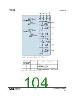
Whenever an analogue input/output is disabled, it remains connected to AVDD/2 through a resistor.
This helps to prevent pop noise when the output is re-enabled. The resistance between the voltage
buffer and the output pins can be controlled using the VROI control bits. The default impedance is
low, so that any capacitors on the outputs can charge up quickly at start-up. If high impedance is
desired for disabled outputs, VROI can then be set to 1, increasing the resistance to about 30kΩ.
There are individual VROI bits for each output or output pair. This allows matching of the rise times
of the outputs if they are driving different capacitors. Using the small resistance with a capacitor for
headphone outputs (typically 220uF) and the larger resistance with a line load capacitance (10uF for
example); will allow both sets of outputs to power up in around the same time, around 200ms.
REGISTER
ADDRESS
BIT
LABEL
DEFAULT
DESCRIPTION
R8 (08h)
13
VBUF_ENA
0
Forces ON the tie-off amplifiers
0 = disabled
Power Mgmt
1
1 = enabled
R76 (4Ch)
8
9
OUT1_VROI
OUT2_VROI
0
0
VREF (AVDD/2) to OUT1L/OUT1R
resistance
Output
Control
0 = approx 500Ω
1 = approx 30 kΩ
VREF (AVDD/2) to OUT2L/OUT2R
resistance
0 = approx 500Ω
1 = approx 30 kΩ
10
11
OUT3_VROI
OUT4_VROI
0
0
VREF (AVDD/2) to OUT3 resistance
0 = approx 500Ω
1 = approx 30 kΩ
VREF (AVDD/2) to OUT4 resistance
0 = approx 500Ω
1 = approx 30 kΩ
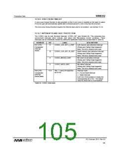
Table 52 Disabled Outputs to VREF Resistance
A dedicated buffer is available for tying off unused analogue I/O pins as shown below. This buffer
can be enabled using the VBUF_ENA register bit.
PD, February 2011, Rev 4.4
103
w

 WOLFSON [ WOLFSON MICROELECTRONICS PLC ]