WM8325
Production Data
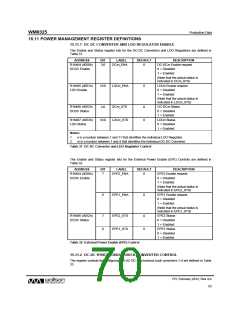
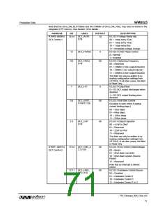
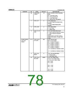
DESCRIPTION
ADDRESS
BIT
LABEL
DEFAULT
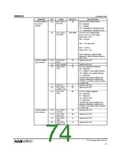
R16474 (405Ah)
DC1_DVS_S
RC [1:0]
DC-DC1 DVS Control Source
00 = Disabled
12:11
00
DC1 DVS
Control
01 = Enabled
10 = Controlled by Hardware DVS1
11 = Controlled by Hardware DVS2
DC-DC1 DVS Voltage select
0.6V to 1.8V in 12.5mV steps
00h to 08h = 0.6V
DC1_DVS_V
SEL [6:0]
6:0
000_0000
09h = 0.6125V
…
48h = 1.4V (see note)
…
67h = 1.7875V
68h to 7Fh = 1.8V
Note - Maximum output voltage
selection in 4MHz switching mode is
48h (1.4V).
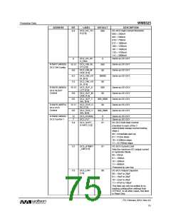
R16475 (405Bh)
DC2 Control 1
DC2_RATE
[1:0]
Same as DC-DC1
15:14
10
DC2_PHASE
Same as DC-DC1
12
0
DC2_FREQ
[1:0]
DC-DC2 Switching Frequency
00 = Reserved
9:8
00
01 = 2.0MHz (2.2uH output inductor)
10 = 4.0MHz (1uH output inductor)
11 = Reserved
This field can only be written to by
loading configuration settings from
OTP/ICE. In all other cases, this field
is Read Only.
DC2_FLT
Same as DC-DC1
Same as DC-DC1
7
0
DC2_SOFT_
START [1:0]
5:4
00
DC2_CAP
[1:0]
DC-DC2 Output Capacitor
00 = Reserved
1:0
00
01 = Reserved
10 = 22uF to 47uF
11 = Reserved
This field can only be written to by
loading configuration settings from
OTP/ICE. In all other cases, this field
is Read Only.
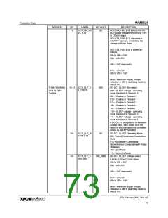
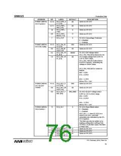
R16476 (405Ch)
DC2 Control 2
DC2_ERR_A
CT [1:0]
Same as DC-DC1
Same as DC-DC1
Same as DC-DC1
Same as DC-DC1
15:14
12:11
10
00
00
0
DC2_HWC_
SRC [1:0]
DC2_HWC_
VSEL
9:8
DC2_HWC_
MODE [1:0]
11
PD, February 2012, Rev 4.0
74
w

 WOLFSON [ WOLFSON MICROELECTRONICS PLC ]