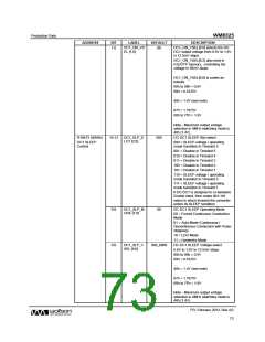
Production Data
WM8325
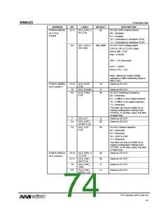
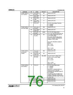
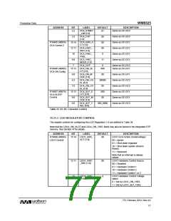
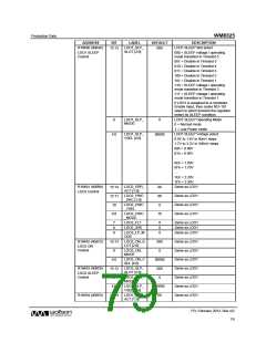
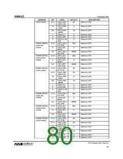
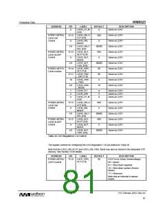
ADDRESS
BIT
LABEL
DEFAULT
DESCRIPTION
Same as DC-DC3
DC4_STNBY
_LIM [1:0]
3:2
01
DC4_CAP
[1:0]
Same as DC-DC3
Same as DC-DC1
Same as DC-DC1
Same as DC-DC1
Same as DC-DC1
1:0
15:14
12:11
10
00
00
00
0
R16485 (4065h)
DC4 Control 2
DC4_ERR_A
CT [1:0]
DC4_HWC_
SRC [1:0]
DC4_HWC_
VSEL
DC4_HWC_
MODE [1:0]
9:8
11
DC4_OVP
Same as DC-DC3
Same as DC-DC1
7
0
R16486 (4066h)
DC4 ON Config
DC4_ON_SL
OT [2:0]
15:13
000
DC4_ON_M
ODE [1:0]
Same as DC-DC1
Same as DC-DC3
Same as DC-DC3
Same as DC-DC1
Same as DC-DC1
Same as DC-DC3
9:8
6:2
00
00000
00
DC4_ON_VS
EL [6:2]
DC4_ON_VS
EL [1:0]
1:0
R16487 (4067h)
DC4_SLP_S
LOT [2:0]
15:13
9:8
000
DC4 SLEEP
Control
DC4_SLP_M
ODE [1:0]
00
DC4_SLP_V
SEL [6:0]
6:0
000_0000
Table 33 DC-DC Converter Control
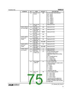
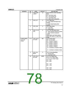
15.11.3 LDO REGULATOR CONTROL
The register controls for configuring the LDO Regulators 1-6 are defined in Table 34.
Note that the LDOn_ON_SLOT and LDOn_ON_VSEL fields may also be stored in the integrated OTP
memory. See Section 14 for details.
ADDRESS
R16488 (4068h)
LDO1 Control
BIT
LABEL
DEFAULT
DESCRIPTION
LDO1 Error Action (Undervoltage)
00 = Ignore
15:14
LDO1_ERR_
ACT [1:0]
00
01 = Shut down regulator
10 = Shut down system (Device
Reset)
11 = Reserved
Note that an Interrupt is always
raised.
LDO1_HWC
_SRC [1:0]
LDO1 Hardware Control Source
00 = Disabled
12:11
00
01 = Hardware Control 1
10 = Hardware Control 2
11 = Hardware Control 1 or 2
LDO1_HWC
_VSEL
LDO1 Hardware Control Voltage
select
10
0
0 = Set by LDO1_ON_VSEL
1 = Set by LDO1_SLP_VSEL
PD, February 2012, Rev 4.0
77
w

 WOLFSON [ WOLFSON MICROELECTRONICS PLC ]