WM8321
Production Data
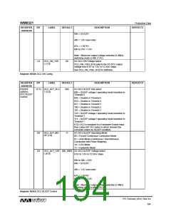
REFER TO
REGISTER
ADDRESS
BIT
LABEL
DEFAULT
DESCRIPTION
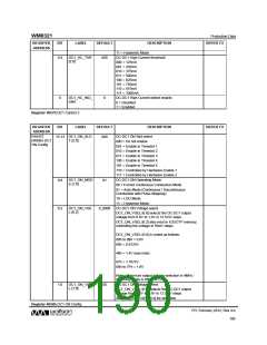
09h = 0.6125V
…
48h = 1.4V (see note)
…
67h = 1.7875V
68h to 7Fh = 1.8V
Note - Maximum output voltage selection in 4MHz
switching mode is 48h (1.4V).
DC2_ON_VSE
L [1:0]
DC-DC2 ON Voltage select
1:0
00
DC2_ON_VSEL [6:0] selects the DC-DC2 output
voltage from 0.6V to 1.8V in 12.5mV steps.
See DC2_ON_VSEL [6:2] for definition.
Register 405Dh DC2 ON Config
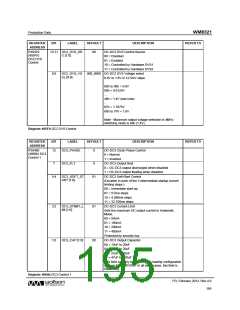
REGISTER
ADDRESS
BIT
LABEL
DEFAULT
DESCRIPTION
REFER TO
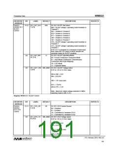
R16478
(405Eh)
DC2 SLEEP
Control
DC2_SLP_SLO
T [2:0]
DC-DC2 SLEEP Slot select
15:13
000
000 = SLEEP voltage / operating mode transition in
Timeslot 5
001 = Disable in Timeslot 5
010 = Disable in Timeslot 4
011 = Disable in Timeslot 3
100 = Disable in Timeslot 2
101 = Disable in Timeslot 1
110 = SLEEP voltage / operating mode transition in
Timeslot 3
111 = SLEEP voltage / operating mode transition in
Timeslot 1
If DC-DC2 is assigned to a Hardware Enable Input,
then codes 001-101 select in which timeslot the
converter enters its SLEEP condition.
DC2_SLP_MO
DE [1:0]
DC-DC2 SLEEP Operating Mode
9:8
6:0
11
00 = Forced Continuous Conduction Mode
01 = Auto Mode (Continuous / Discontinuous
Conduction with Pulse-Skipping)
10 = LDO Mode
11 = Hysteretic Mode
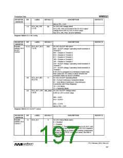
DC2_SLP_VSE
L [6:0]
DC-DC2 SLEEP Voltage select
0.6V to 1.8V in 12.5mV steps
000_0000
00h to 08h = 0.6V
09h = 0.6125V
…
48h = 1.4V (see note)
…
67h = 1.7875V
68h to 7Fh = 1.8V
Note - Maximum output voltage selection in 4MHz
switching mode is 48h (1.4V).
Register 405Eh DC2 SLEEP Control
PD, February 2012, Rev 4.0
194
w

 WOLFSON [ WOLFSON MICROELECTRONICS PLC ]