WM8321
Production Data
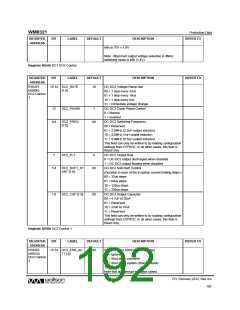
REFER TO
REGISTER
ADDRESS
BIT
LABEL
DEFAULT
DESCRIPTION
68h to 7Fh = 1.8V
Note - Maximum output voltage selection in 4MHz
switching mode is 48h (1.4V).
Register 405Ah DC1 DVS Control
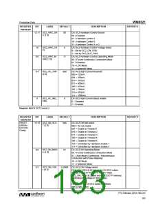
REGISTER
ADDRESS
BIT
LABEL
DEFAULT
DESCRIPTION
REFER TO
R16475
(405Bh)
DC2 Control
1
DC2_RATE
[1:0]
DC-DC2 Voltage Ramp rate
00 = 1 step every 32us
15:14
10
01 = 1 step every 16us
10 = 1 step every 8us
11 = Immediate voltage change
DC-DC2 Clock Phase Control
0 = Normal
DC2_PHASE
12
1
1 = Inverted
DC2_FREQ
[1:0]
DC-DC2 Switching Frequency
00 = Reserved
9:8
00
01 = 2.0MHz (2.2uH output inductor)
10 = 4.0MHz (1uH output inductor)
11 = 4.0MHz (0.5uH output inductor)
This field can only be written to by loading configuration
settings from OTP/ICE. In all other cases, this field is
Read Only.
DC2_FLT
DC-DC2 Output float
7
0
0 = DC-DC2 output discharged when disabled
1 = DC-DC2 output floating when disabled
DC-DC2 Soft-Start Control
(Duration in each of the 8 startup current limiting steps.)
00 = 32us steps
DC2_SOFT_ST
ART [1:0]
5:4
00
01 = 64us steps
10 = 128us steps
11 = 256us steps
DC2_CAP [1:0]
DC-DC2 Output Capacitor
00 = 4.7uF to 20uF
1:0
00
01 = Reserved
10 = 22uF to 47uF
11 = Reserved
This field can only be written to by loading configuration
settings from OTP/ICE. In all other cases, this field is
Read Only.
Register 405Bh DC2 Control 1
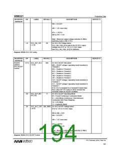
REGISTER
ADDRESS
BIT
LABEL
DEFAULT
DESCRIPTION
REFER TO
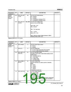
R16476
(405Ch)
DC2 Control
2
DC2_ERR_AC
T [1:0]
DC-DC2 Error Action (Undervoltage)
00 = Ignore
15:14
00
01 = Shut down converter
10 = Shut down system (Device Reset)
11 = Reserved
Note that an Interrupt is always raised.
PD, February 2012, Rev 4.0
192
w

 WOLFSON [ WOLFSON MICROELECTRONICS PLC ]