Production Data
WM8321
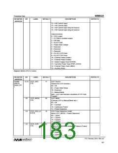
REGISTER
ADDRESS
BIT
LABEL
DEFAULT
DESCRIPTION
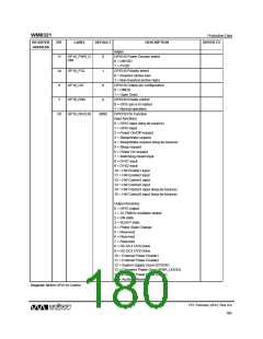
12 = HW Control1 input
REFER TO
13 = HW Control2 input
14 = HW Control1 input (long de-bounce)
15 = HW Control2 input (long de-bounce)
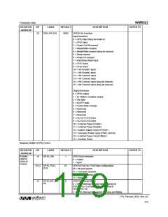
Output functions:
0 = GPIO output
1 = 32.768kHz oscillator output
2 = ON state
3 = SLEEP state
4 = Power State Change
5 = Reserved
6 = Reserved
7 = Reserved
8 = DC-DC1 DVS Done
9 = DC-DC2 DVS Done
10 = External Power Enable1
11 = External Power Enable2
12 = System Supply Good (SYSOK)
13 = Converter Power Good (PWR_GOOD)
14 = External Power Clock (2MHz)
15 = Auxiliary Reset
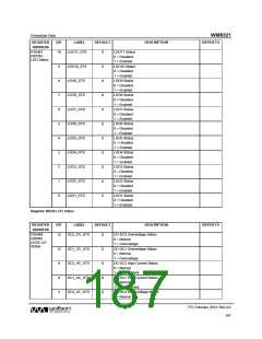
Register 4043h GPIO12 Control
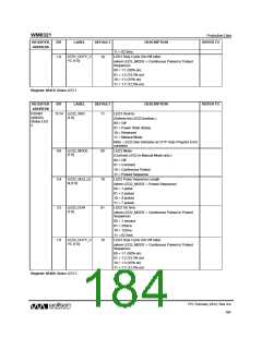
REGISTER
ADDRESS
BIT
LABEL
DEFAULT
DESCRIPTION
REFER TO
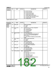
R16460
(404Ch)
Status LED
1
LED1_SRC
[1:0]
LED1 Source
15:14
11
(Selects the LED1 function.)
00 = Off
01 = Power State Status
10 = Reserved
11 = Manual Mode
Note - LED1 also indicates completion of OTP Auto
Program
LED1_MODE
[1:0]
LED1 Mode
9:8
5:4
3:2
00
10
01
(Controls LED1 in Manual Mode only.)
00 = Off
01 = Constant
10 = Continuous Pulsed
11 = Pulsed Sequence
LED1 Pulse Sequence Length
(when LED1_MODE = Pulsed Sequence)
00 = 1 pulse
LED1_SEQ_LE
N [1:0]
01 = 2 pulses
10 = 4 pulses
11 = 7 pulses
LED1_DUR
[1:0]
LED1 On time
(when LED1_MODE = Continuous Pulsed or Pulsed
Sequence)
00 = 1 second
01 = 250ms
10 = 125ms
PD, February 2012, Rev 4.0
183
w

 WOLFSON [ WOLFSON MICROELECTRONICS PLC ]