Production Data
WM8321
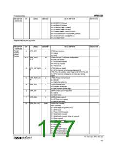
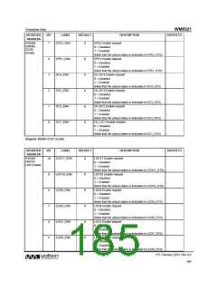
REGISTER
ADDRESS
BIT
LABEL
DEFAULT
DESCRIPTION
REFER TO
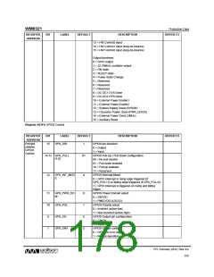
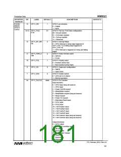
R16450
(4042h)
GPIO11
Control
GP11_DIR
GPIO11 pin direction
0 = Output
15
1
1 = Input
GP11_PULL
[1:0]
GPIO11 Pull-Up / Pull-Down configuration
00 = No pull resistor
14:13
01
01 = Pull-down enabled
10 = Pull-up enabled
11 = Reserved
GP11_INT_MO
DE
GPIO11 Interrupt Mode
12
0
0 = GPIO interrupt is rising edge triggered (if
GP11_POL=1) or falling edge triggered (if
GP11_POL=0)
1 = GPIO interrupt is triggered on rising and falling
edges
GP11_PWR_D
OM
GPIO11 Power Domain select
0 = DBVDD
11
10
9
0
1
1 = PVDD
GP11_POL
GP11_OD
GPIO11 Polarity select
0 = Inverted (active low)
1 = Non-Inverted (active high)
GPIO11 Output pin configuration
0 = CMOS
0
1 = Open Drain
GP11_ENA
GP11_FN [3:0]
GPIO11 Enable control
0 = GPIO pin is tri-stated
1 = Normal operation
7
0
GPIO11 Pin Function
3:0
0000
Input functions:
0 = GPIO input (long de-bounce)
1 = GPIO input
2 = Power On/Off request
3 = Sleep/Wake request
4 = Sleep/Wake request (long de-bounce)
5 = Sleep request
6 = Power On request
7 = Watchdog Reset input
8 = DVS1 input
9 = DVS2 input
10 = HW Enable1 input
11 = HW Enable2 input
12 = HW Control1 input
13 = HW Control2 input
14 = HW Control1 input (long de-bounce)
15 = HW Control2 input (long de-bounce)
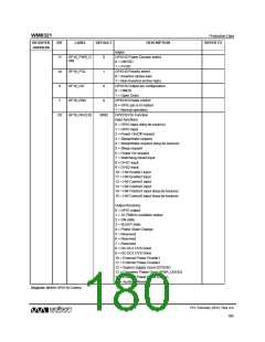
Output functions:
0 = GPIO output
1 = 32.768kHz oscillator output
2 = ON state
3 = SLEEP state
4 = Power State Change
5 = Reserved
6 = Reserved
7 = Reserved
PD, February 2012, Rev 4.0
181
w

 WOLFSON [ WOLFSON MICROELECTRONICS PLC ]