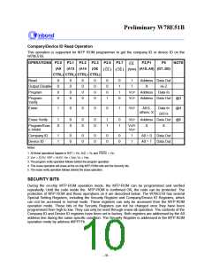
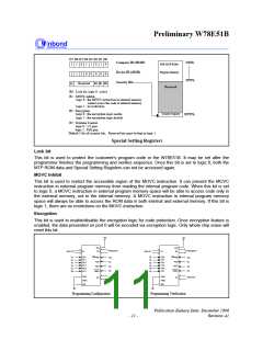
Preliminary W78E51B
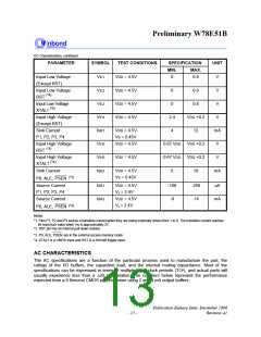
DC Characteristics, continued
PARAMETER
SYMBOL
TEST CONDITIONS
SPECIFICATION
UNIT
V
MIN.
MAX.
Input Low Voltage
(Except RST)
Input Low Voltage
RST (*4)
VIL1
VIL2
VIL3
VIH1
ISK1
VIH2
VIH3
ISK2
VDD = 4.5V
VDD = 4.5V
VDD = 4.5V
VDD = 4.5V
0
0.8
0
0.8
0.8
V
Input Low Voltage
XTAL1 (*4)
0
V
Input High Voltage
(Except RST)
Sink Current
2.4
VDD +0.2
12
V
VDD = 4.5V
Vs = 0.45V
VDD = 4.5V
4
mA
V
P1, P2, P3, P4
Input High Voltage
RST (*4)
0.67 VDD
0.67 VDD
8
VDD +0.2
VDD +0.2
16
Input High Voltage
XTAL1 (*4)
VDD = 4.5V
V
Sink Current
VDD = 4.5V
Vs = 0.45V
mA
(*3)
P0, ALE, PSEN
Source Current
P1, P2, P3, P4
Source Current
ISR1
ISR2
VDD = 4.5V
VS = 2.4V
VDD = 4.5V
Vs = 2.4V
-100
-8
-250
-14
uA
mA
(*3)
P0, ALE, PSEN
Notes:
*1. Pins P1, P2 and P3 source a transition current when they are being externally driven from 1 to 0. The transition current reaches
its maximum value when VIN is approximately 2V.
*2. RST pin has an internal pull-down resistor.
*3. P0, ALE, PSEN are in the external access memory mode.
*4. XTAL1 is a CMOS input and RST is a Schmitt trigger input.
AC CHARACTERISTICS
The AC specifications are a function of the particular process used to manufacture the part, the
ratings of the I/O buffers, the capacitive load, and the internal routing capacitance. Most of the
specifications can be expressed in terms of multiple input clock periods (TCP), and actual parts will
usually experience less than a ±20 nS variation. The numbers below represent the performance
expected from a 0.6micron CMOS process when using 2 and 4 mA output buffers.
Publication Release Date: December 1998
- 13 -
Revision A1

 WINBOND [ WINBOND ]