Preliminary W78E51B
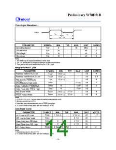
Clock Input Waveform
XTAL1
T
CH
T
CL
F
T
CP
OP,
PARAMETER
Operating Speed
SYMBOL
FOP
MIN.
0
TYP.
MAX.
UNIT
MHz
nS
NOTES
-
-
-
-
40
-
1
2
3
3
Clock Period
Clock High
Clock Low
Notes:
TCP
25
10
10
TCH
-
nS
TCL
-
nS
1. The clock may be stopped indefinitely in either state.
2. The TCP specification is used as a reference in other specifications.
3. There are no duty cycle requirements on the XTAL1 input.
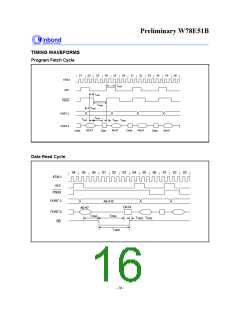
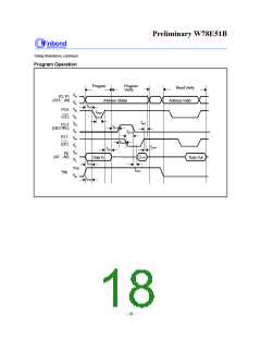
Program Fetch Cycle
PARAMETER
SYMBOL
TAAS
MIN.
TYP.
MAX.
UNIT
nS
NOTES
Address Valid to ALE Low
Address Hold from ALE Low
-
-
-
-
-
-
4
1, 4
4
1 TCP -D
1 TCP -D
1 TCP -D
-
TAAH
nS
TAPL
nS
ALE Low to PSEN Low
PSEN Low to Data Valid
Data Hold after PSEN High
TPDA
-
2 TCP
nS
2
3
TPDH
TPDZ
TALW
TPSW
0
0
-
1 TCP
nS
nS
nS
nS
-
1 TCP
Data Float after PSEN High
ALE Pulse Width
2 TCP
3 TCP
-
-
4
4
2 TCP -D
3 TCP -D
PSEN Pulse Width
Notes:
1. P0.0- P0.7, P2.0- P2.7 remain stable throughout entire memory cycle.
2. Memory access time is 3 TCP.
3. Data have been latched internally prior to PSEN going high.
4. "D" (due to buffer driving delay and wire loading) is 20 nS.
Data Read Cycle
PARAMETER
ALE Low to RD Low
RD Low to Data Valid
Data Hold from RD High
Data Float from RD High
RD Pulse Width
SYMBOL
MIN.
TYP.
MAX.
UNIT
nS
NOTES
1, 2
TDAR
-
3 TCP -D
3 TCP +D
4 TCP
2 TCP
2 TCP
-
TDDA
TDDH
TDDZ
TDRD
-
-
nS
1
0
0
-
-
nS
nS
6 TCP
nS
2
6 TCP -D
Notes:
1. Data memory access time is 8 TCP.
2. "D" (due to buffer driving delay and wire loading) is 20 nS.
- 14 -

 WINBOND [ WINBOND ]