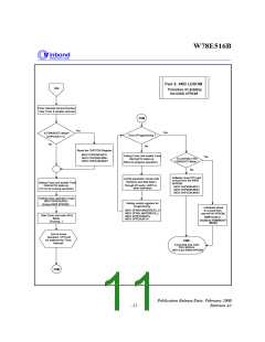
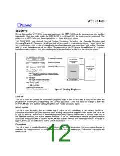
W78E516B
AC CHARACTERISTICS
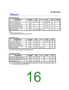
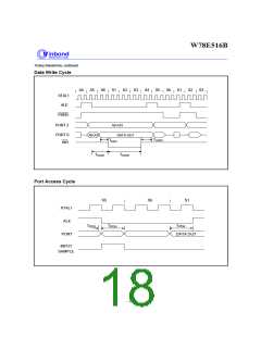
The AC specifications are a function of the particular process used to manufacture the part, the
ratings of the I/O buffers, the capacitive load, and the internal routing capacitance. Most of the
CP
specifications can be expressed in terms of multiple input clock periods (T ), and actual parts will
±
usually experience less than a 20 nS variation. The numbers below represent the performance
expected from a 0.6 micron CMOS process when using 2 and 4 mA output buffers.
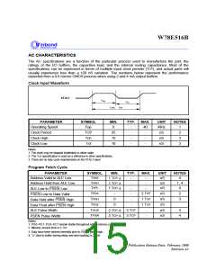
Clock Input Waveform
XTAL1
TCH
TCL
FOP,
TCP
PARAMETER
Operating Speed
Clock Period
SYMBOL
Fop
MIN.
0
TYP.
MAX.
UNIT
MHz
nS
NOTES
-
-
-
-
40
-
1
2
3
3
TCP
Tch
25
10
10
Clock High
-
nS
Clock Low
Tcl
-
nS
Notes:
1. The clock may be stopped indefinitely in either state.
2. The TCP specification is used as a reference in other specifications.
3. There are no duty cycle requirements on the XTAL1 input.
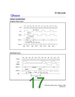
Program Fetch Cycle
PARAMETER
SYMBOL
MIN.
TYP.
MAX.
UNIT
nS
NOTES
AAS
T
Address Valid to ALE Low
Address Hold from ALE Low
-
-
-
-
-
-
4
1, 4
4
CP
1 T
D
D
D
-
-
-
AAH
T
CP
nS
1 T
1 T
APL
T
nS
CP
PSEN
ALE Low to
Low
PDA
CP
T
-
-
-
-
2 T
nS
nS
nS
nS
nS
2
3
PSEN
Low to Data Valid
PDH
CP
1 T
T
0
PSEN
PSEN
Data Hold after
Data Float after
High
High
PDZ
T
CP
1 T
0
ALW
CP
ALE Pulse Width
PSEN
T
2 T
-
-
4
4
CP
D
2 T
-
PSW
CP
T
CP
3 T -D
3 T
Pulse Width
Notes:
1. P0.0 P0.7, P2.0 P2.7 remain stable throughout entire memory cycle.
-
-
2. Memory access time is 3 TCP.
3. Data have been latched internally prior to
going high.
PSEN
4. " " (due to buffer driving delay and wire loading) is 20 nS.
D
Publication Release Date: February 2000
Revision A3
- 15 -

 WINBOND [ WINBOND ]