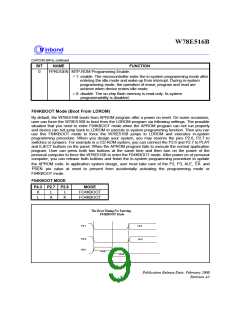
W78E516B
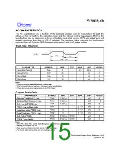
Oscillator Control
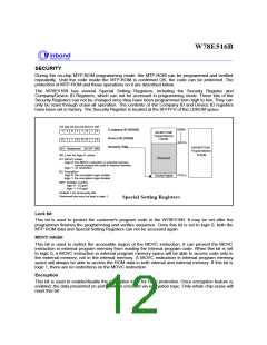
W78E516B/E516 allow user to diminish the gain of on-chip oscillator amplifier by using programmer
to set the bit B7 of security register. Once B7 is set to 0, a half of gain will be decreased. Care must
be taken if user attempts to diminish the gain of oscillator amplifier, reducing a half of gain may
improperly affect the external crystal operation at high frequency above 24 MHz. The value of R and
C1, C2 may need some adjustment while running at lower gain.
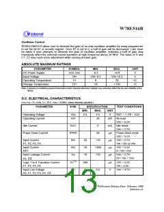
ABSOLUTE MAXIMUM RATINGS
PARAMETER
DC Power Supply
SYMBOL
MIN.
-0.3
SS
MAX.
+6.0
DD
UNIT
V
DD
V
SS
V
-
IN
V
Input Voltage
V
-0.3
V
+0.3
V
A
Operating Temperature
Storage Temperature
T
0
70
°
C
C
ST
T
-55
+150
°
Note: Exposure to conditions beyond those listed under Absolute Maximum Ratings may adversely affect the life and reliability of the
device.
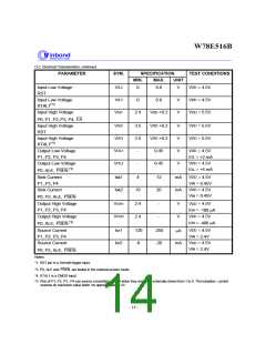
D.C. ELECTRICAL CHARACTERISTICS
(VDD-VSS = 5V 10%, TA = 25 C, Fosc = 20 MHz, unless otherwise specified.)
±
°
PARAMETER
SYM.
SPECIFICATION
TEST CONDITIONS
MIN.
MAX.
UNIT
DD
DD
Operating Voltage
V
4.5
-
5.5
20
V
RST = 1, P0 = V
DD
Operating Current
I
mA
No load
DD
V
= 5.5V
IDLE
Idle Current
I
-
6
mA
Idle mode
DD
V
= 5.5V
PWDN
Power Down Current
I
-
50
Power-down mode
mA
DD
V
V
V
V
= 5.5V
= 5.5V
IN1
IN2
LK
DD
IN
Input Current
P1, P2, P3, P4
Input Current
RST
I
-50
-10
-10
+10
+300
+10
m
A
DD
= 0V or V
DD
I
= 5.5V
m
A
IN
DD
0< V <V
DD
V
Input Leakage Current
I
= 5.5V
m
A
IN
DD
0V< V < V
EA
P0,
[*4]
TL
DD
Logic 1 to 0 Transition Current
P1, P2, P3, P4
I
-500
0
-
V
V
V
= 5.5V
m
A
IN
DD
= 2.0V
IL1
Input Low Voltage
V
0.8
V
= 4.5V
EA
P0, P1, P2, P3, P4,
Publication Release Date: February 2000
Revision A3
- 13 -

 WINBOND [ WINBOND ]