I5216 SERIES
Advanced Information
PRELIMINARY
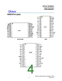
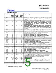
PIN DESCRIPTION
Pin Name
Pin No. Pin No. Pin No. Functionality
28-pin
TSOP
28-pin
PDIP
28-pin
SOIC
RAC
/INT
4
25
25
Row Address Clock; an open drain output. The RAC pin goes LOW
TRACLO before the end of each row of memory, and returns HIGH
at exactly the end of each row of memory.
Interrupt Output; an open drain output indicating that a set EOM bit
has been found during Playback, or that the chip is in an Overflow
(OVF) condition. This pin remains LOW until a Read Status
command is executed.
1
5
26
26
MCLK
6
27
27
This pin allows the internal clock of the Voice record/playback
system to be externally driven for enhanced timing precision. This
pin is grounded for most applications. It is required for the CODEC
operation.
SCL
SDA
9
2
4
2
4
Serial Clock Line is part of the I2C serial bus. It is used to clock the
data into and out of the I2C interface.
11
Serial Data Line is part of the I2C serial bus. Data is passed
between devices on the bus over this line.
A0
A1
12
10
16
17
18
19
22
20
5
3
9
10
11
12
15
13
7
3
10
9
Input pin that supplies the LSB for the I2C Slave Address.
Input pin that supplies the LSB +1 bit for the I2C Slave Address.
Differential positive Input to the microphone amplifier.
Differential negative Input to the microphone amplifier.
Microphone Bias Voltage
AGC Capacitor connection. Required for the on-chip AGC amplifier.
Differential Positive Speaker Driver Output.
Differential Negative Speaker Driver Output. When the speaker
outputs are in use, the AUX OUT output is disabled.
Auxiliary Input. This is one of the gain adjustable analog inputs for
the device.
MIC+
MIC-
MICBS
ACAP
SP+
8
12
15
13
SP-
AUX IN
24
25
17
18
17
20
AUX OUT
Auxiliary Output. This is one the analog outputs for the device.
When this output is in use, the SP+ and SP- outputs are disabled.
Serial Digital Audio PCM Input.
SDI
SDIO
WS
SCK
VCCD
2
3
28
27
7,8
23
24
21
20
1,28
22
24
18
19
1,28
Serial Digital Audio PCM Output or I2S Input/Output.
Digital audio PCM Frame sync (FS) or I2S Word Sync (WS).
Digital audio PCM or I2S Serial Clock.
Positive Digital Supply pins. These pins carry noise generated by
internal clocks in the chip. They must be carefully bypassed to
Digital Ground to ensure correct device operation.
Digital Ground pins.
VSSD
VSSA
VCCA
13,14
1,15,21
23
6,7
5,6
8,14,22 11,14,23 Analog Ground pins.
16
16
Positive Analog Supply pin. This pin supplies the low level audio
sections for the device. It should be carefully bypassed to Analog
Ground to ensure correct device operation.
No Connection
NC
26
19
21
1 See parameters section of the datasheet.
Publication Release Date: November 30, 2001
-5
Revision A1

 WINBOND [ WINBOND ]