I5216 SERIES
Advanced Information
PRELIMINARY
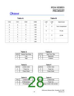
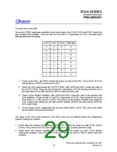
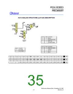
3. Select the INPUT SOURCE MUX (only) to the S1 SUMMING amplifier—Bits S1M0 and S1M1
control the state of the SUM1 SUMMING amplifier. These are bits D7 and D8, respectively, of
CFG1 and they should be set to the state where D7 is ZERO and D8 is ONE to select the INPUT
SOURCE MUX (only) path.
4. Select the SUM1 SUMMING amplifier path through the FILTER MUX—Bit FLS0 controls the state
of the FILTER MUX. This is bit D4 of CFG1 and it must be set to ZERO to select the SUM1
SUMMING amplifier path.
5. Deselect the signal compression-Bit AMT0 controls the signal compression. This is bit D7 of CFG0
and it must be set to ZERO.
6. Power up the LOW PASS FILTER—Bit FLPD controls the power up state of the LOW PASS
FILTER stage. This is bit D1 of CFG1 and it must be set to ZERO to power up the LOW PASS
FILTER STAGE.
7. Select the 5.3 kHz sample rate—Bits FLD0 and FLD1 select the Low Pass filter setting and sample
rate to be used during record and playback. These are bits D2 and D3 of CFG1. To enable the 5.3
kHz sample rate, D2 must be set to ZERO and D3 set to ONE.
8. Select the LOW PASS FILTER input (only) to the S2 SUMMING amplifier – BITS S2M0 and S2M1
control the state of the SUM2 SUMMING amplifier. These are bits D5 and D6, respectively, of
CFG1 and they should be set to the state where D5 is ZERO and D6 is ONE to select the LOW
PASS FILTER (only) path.
9. Power up the Internal Oscillator—Bit OSPD controls the power up state of the Internal Oscillator.
This is bit D8 of CFG0 and it must be set to ZERO to power up the Internal Oscillator.
To set up the chip for Memo Record, the configuration registers are set up as follows:
CFG0=0000 0100 0000 0001 (hex 0401).
CFG1=0000 0001 0100 1000 (hex 0148).
CFG2=0000 0000 0000 0011 (hex 0003).
Only those portions necessary for this mode are powered up.
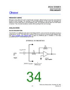
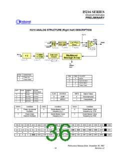
MEMO AND CALL PLAYBACK
This mode sets the chip up for local playback of messages that were recorded earlier. The playback
path is from the MULTILEVEL STORAGE ARRAY to the FILTER MUX, then to the LOW PASS
FILTER stage. From there, the audio path goes through the SUM2 SUMMING amplifier to the
VOLUME MUX, through the VOLUME CONTROL then to the SPEAKER output stage. We will assume
that we are driving a piezo speaker element and that this audio was previously recorded at 8 kHz. All
unnecessary stages will be powered down.
1. Select the MULTILEVEL STORAGE ARRAY path through the FILTER MUX—Bit FLS0, the state
of the FILTER MUX. This is bit D4 of CFG1 and must be set to ONE to select the MULTILEVEL
STORAGE ARRAY.
Publication Release Date: November 30, 2001
- 32
Revision A1

 WINBOND [ WINBOND ]