W3EG7236S-D3
White Electronic Designs
PRELIMINARY
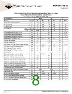
DDR SDRAM COMPONENT ELECTRICAL CHARACTERISTICS AND
RECOMMENDED AC OPERATING CONDITIONS
0°C ≤ TA ≤ +70°C; VCC = +2.5V 0.2V, VCCQ = +2.5V 0.2V
AC Characteristics
262/265
202
Parameter
Symbol
tAC
Min
-0.75
0.45
0.45
7.5
Max
+0.75
0.55
0.55
13
Min
-0.8
0.45
0.45
8
Max
+0.8
0.55
0.55
13
Units
ns
tCK
tCK
ns
ns
ns
ns
ns
ns
tCK
tCK
ns
tCK
tCK
tCK
ns
ns
ns
ns
ns
ns
ns
ns
ns
ns
ns
ns
ns
ns
ns
Notes
Access window of DQs from CK, CK#
CK high-level width
CK low-level width
tCH
16
16
tCL
Clock cycle time
CL=2.5
CL=2
tCK (2.5)
tCK (2)
tDH
22
7.5/10
0.5
13
10
13
22
DQ and DM input hold time relative to DQS
DQ and DM input setup time relative to DQS
DQ and DM input pulse width (for each input)
Access window of DQS from CK, CK#
DQS input high pulse width
0.6
0.6
2
14,17
14,17
17
tDS
0.5
tDIPW
tDQSCK
tDQSH
tDQSL
tDQSQ
tDQSS
tDSS
tDSH
tHP
1.75
-0.75
0.35
0.35
+0.75
-0.8
0.35
0.35
+0.8
DQS input low pulse width
DQS-DQ skew, DQS to last DQ valid, per group, per access
Write command to first DQS latching transition
DQS falling edge to CK rising - setup time
DQS falling edge from CK rising - hold time
Half clock period
0.5
0.6
13,14
0.75
0.2
1.25
0.75
0.2
1.25
0.2
0.2
tCH, tCL
tCH, tCL
18
8,19
8,20
6
Data-out high-impedance window from CK, CK#
Data-out low-impedance window from CK, CK#
Address and control input hold time (fast slew rate)
Address and control input set-up time (fast slew rate)
Address and control input hold time (slow slew rate)
Address and control input setup time (slow slew rate)
Address and control input pulse width (for each input)
LOAD MODE REGISTER command cycle time
DQ-DQS hold, DQS to first DQ to go non-valid, per access
Data hold skew factor
tHZ
+0.75
+0.8
tLZ
-0.75
0.90
0.90
1
-0.8
1.1
1.1
1.1
1.1
2.2
16
tIHf
tISf
6
tIHs
6
tISs
1
6
tIPW
2.2
15
tMRD
tQH
tHP-tQHS
tHP-tQHS
13,14
15
tQHS
tRAS
tRAP
tRC
0.75
120,000
1
120,000
ACTIVE to PRECHARGE command
40
20
65
75
40
20
70
80
ACTIVE to READ with Auto precharge command
ACTIVE to ACTIVE/AUTO REFRESH command period
AUTO REFRESH command period
tRFC
21
November 2004
Rev. 1
8
White Electronic Designs Corporation • (602) 437-1520 • www.wedc.com

 WEDC [ WHITE ELECTRONIC DESIGNS CORPORATION ]