W3EG7236S-D3
White Electronic Designs
PRELIMINARY
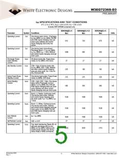
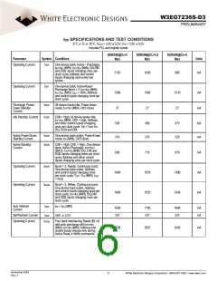
IDD SPECIFICATIONS AND TEST CONDITIONS
0°C ≤ TA ≤ 70°C, VCCQ = 2.5V 0.2V, VCC = 2.5V 0.2V
Includes DDR SDRAM component only
DDR266@CL=2
Max
DDR266@CL=2.5
DDR200@CL=2
Parameter
Symbol Conditions
IDD0
Units
Max
Max
Operating Current
One device bank; Active - Precharge;
tRC=tRC (MIN); tCK=tCK (MIN); DQ,DM
and DQS inputs changing once per
clock cycle; Address and control
inputs changing once every two
cycles.
810
720
675
mA
Operating Current
IDD1
One device bank; Active-Read-
Precharge Burst = 2; tRC=tRC (MIN);
tCK=tCK (MIN); lOUT = 0mA; Address
and control inputs changing once per
clock cycle.
1080
27
990
27
900
27
mA
rnA
Precharge Power-
Down Standby
Current
IDD2P
All device banks idle; Power-down
mode; tCK=tCK (MIN); CKE=(low)
Idle Standby Current
IDD2F
CS# = High; All device banks idle;
tCK=tCK (MIN); CKE = high; Address
and other control inputs changing
once per clock cycle. VIN = VREF for
DQ, DQS and DM.
225
315
180
270
162
225
mA
mA
Active Power-Down
Standby Current
IDD3P
IDD3N
One device bank active; Power-Down
mode; tCK (MIN); CKE=(low)
Active Standby
Current
CS# = High; CKE = High; One device
bank; Active-Precharge; tRC=tRAS
(MAX); tCK=tCK (MIN); DQ, DM and
DQS inputs changing twice per clock
cycle; Address and other control
inputs changing once per clock cycle.
495
1530
1530
405
1260
1260
360
1080
1035
mA
mA
rnA
Operating Current
Operating Current
IDD4R
Burst = 2; Reads; Continuous burst;
One device bank active; Address
and control inputs changing once
per clock cycle; TCK= TCK (MIN); lOUT
= 0mA.
IDD4W
Burst = 2; Writes; Continuous burst;
One device bank active; Address
and control inputs changing once per
clock cycle; tCK=tCK (MIN); DQ,DM
and DQS inputs changing once per
clock cycle.
Auto Refresh
Current
IDD5
tRC = tRC (MIN)
1620
27
1485
27
1350
27
mA
mA
Self Refresh Current
Operating Current
IDD6
CKE ≤ 0.2V
IDD7A
Four bank interleaving Reads (BL=4)
with auto precharge with tRC=tRC
(MIN); tCK=tCK (MIN); Address and
control inputs change only during
Active Read or Write commands.
2925
2520
2115
mA
November 2004
Rev. 1
5
White Electronic Designs Corporation • (602) 437-1520 • www.wedc.com

 WEDC [ WHITE ELECTRONIC DESIGNS CORPORATION ]