W3EG7236S-D3
White Electronic Designs
PRELIMINARY
Notes
1.
2.
All voltages referenced to VSS
11. It is recommended that DQS be valid (HIGH or LOW) on or before
the WRITE command. The case shown (DQS going from High-Z to
logic LOW) applies when no WRITEs were previously in progress
on the bus. If a previous WRITE was in progress, DQS could be
Tests for AC timing, IDD, and electrical AC and DC characteristics
may be conducted at normal reference / supply voltage levels, but
the related specifications and device operations are guaranteed for
the full voltage range specified.
high during this time, depending on tDQSS
.
12. The refresh period is 64ms. This equates to an average refresh
rate of 15.625µs. However, an AUTO REFRESH command must
be asserted at least once every 140.6µs; burst refreshing or
posting by the DRAM controller greater than eight refresh cycles is
not allowed.
3.
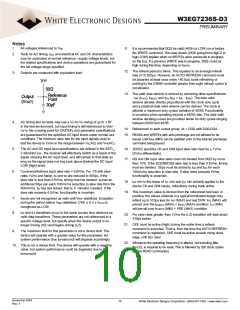
Outputs are measured with equivalent load:
VTT
50ΩΩ
13. The valid data window is derived by achieving other specifications
- tHP (tCK/2), tDQSQ, and tQH (tQH = tHP - tQHS). The data valid
window derates directly proportional with the clock duty cycle
and a practical data valid window can be derived. The clock is
allowed a maximum duty cycled variation of 45/55. Functionality
is uncertain when operating beyond a 45/55 ratio. The data valid
window derating curves are provided below for duty cycles ranging
between 50/50 and 45/55.
RReeffeerreennccee
Outputt
Point
30ppFF
(VOUT
)
4.
AC timing and IDD tests may use a VIL-to-VIH swing of up to 1.5V
in the test environment, but input timing is still referenced to VREF
(or to the crossing point for CK/CK#), and parameter specifications
are guaranteed for the specified AC input levels under normal use
conditions. The minimum slew rate for the input signals used to
test the device is 1V/ns in the range between VIL(AC) and VIH(AC).
14. Referenced to each output group: x4 = DQS with DQ0-DQ4.
15. READs and WRITEs with auto precharge are not allowed to be
issued until tRAS (MIN) can be satisfied prior to the internal precharge
command being issued.
5.
6.
The AC and DC input level specifications are defined in the SSTL_
2 standard (i.e., the receiver will effectively switch as a result of the
signal crossing the AC input level, and will remain in that state as
long as the signal does not ring back above [below] the DC input
LOW [high] level).
16. JEDEC specifies CK and CK# input slew rate must be > 1V/ns
(2V/ns differentially).
17. DQ and DM input slew rates must not deviate from DQS by more
than 10%. If the DQ/DM/DQS slew rate is less than 0.5V/ns, timing
must be derated: 50ps must be added to tDS and tDH for each
100mV/ns reduction in slew rate. If slew rates exceeds 4V/ns,
functionality is uncertain.
Command/Address input slew rate = 0.5V/ns. For -75 with slew
rates 1V/ns and faster, tIS and tIH are reduced to 900ps. If the
slew rate is less than 0.5V/ns, timing must be derated: tIS has an
additional 50ps per each 100mV/ns reduction in slew rate from the
500mV/ns. tIH has 0ps added, that is, it remains constant. If the
slew rate exceeds 4.5V/ns, functionality is uncertain.
18.
t
HP min is the lesser of tCL min and tCH min actually applied to the
device CK and CK# inputs, collectively during bank active.
19. This maximum value is derived from the referenced test load. In
practice, the values obtained in a typical terminated design may
reflect up to 310ps less for tHZ (MAX) and last DVW. tHZ (MAX) will
prevail over the tDQSCK (MAX) + tRPST (MAX) condition. tLZ (MIN)
will prevail over tDQSCK (MIN) + PRE (MAX) condition.
7.
8.
Inputs are not recognized as valid until VREF stabilizes. Exception:
during the period before VREF stabilizes, CKE ≤ 0.3 x VCCQ is
recognized as LOW.
tHZ and tLZ transitions occur in the same access time windows as
20. For slew rates greater than 1V/ns the (LZ) transition will start about
310ps earlier.
valid data transitions. These parameters are not referenced to a
specific voltage level, but specify when the device output is no
longer driving (HZ) and begins driving (LZ).
21. CKE must be active (High) during the entire time a refresh
command is executed. That is, from the time the AUTO REFRESH
command is registered, CKE must be active at each rising clock
edge, until tREF later.
9.
The maximum limit for this parameter is not a device limit. The
device will operate with a greater value for this parameter, but
system performance (bus turnaround) will degrade accordingly.
22. Whenever the operating frequency is altered, not including jitter,
the DLL is required to be reset. This is followed by 200 clock cycles
(before READ commands).
10. This is not a device limit. The device will operate with a negative
value, but system performance could be degraded due to bus
turnaround.
November 2004
Rev. 1
10
White Electronic Designs Corporation • (602) 437-1520 • www.wedc.com

 WEDC [ WHITE ELECTRONIC DESIGNS CORPORATION ]