SCA61T Series
1.7 Electrical Connection
If the SPI interface is not used SCK (pin1), MISO (pin3), MOSI (pin4) and CSB (pin7) must be left
floating. Self-test can be activated applying logic “1” (positive supply voltage level) to ST pin (pin
6). If ST feature is not used pin 6 must be left floating or connected to GND. Inclination signal is
provided from pin OUT.
1 SCK
2 MISO
3 MOSI
8 VDD
7 OUT
6 ST
Figure 3.
SCA61T electrical connection
No.
1
2
3
4
Node
I/O
Input
Output
Input
Supply
Input
Input
Description
Serial clock
Master in slave out; data output
Master out slave in; data input
Ground
Chip select (active low)
Self test input
SCK
MISO
MOSI
GND
CSB
ST
5
6
7
8
Out
VDD
Output
Supply
Output
Positive supply voltage (+5V DC)
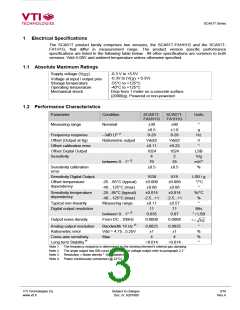
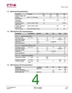
1.8 Typical Performance Characteristics
Typical offset and sensitivity temperature dependencies of SCA61T are presented in following
diagrams. These results represent the typical performance of SCA61T components. The mean
value and 3 sigma limits (mean ± 3× standard deviation) and specification limits are presented in
following diagrams. The 3 sigma limits represents 99.73% of the SCA61T population.
Temperature dependency of SCA61T offset
1.0
specification
0.8
0.6
limit
0.4
0.2
average
+3 sigma
-3 sigma
0.0
-0.2
-0.4
-0.6
-0.8
-1.0
specification
limit
-40
-20
0
20
40
60
80
100
120
Temp [°C]
Figure 4.
Typical temperature dependency of the SCA61T offset
VTI Technologies Oy
www.vti.fi
Subject to changes
Doc. nr. 8261900
6/18
Rev.A

 VTI [ VTI TECHNOLOGIES ]