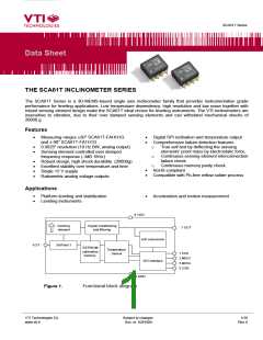
SCA61T Series
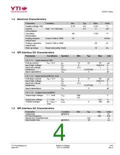
1.6 SPI Interface Timing Specifications
Parameter
Conditions
Symbol
TLS1
Min.
120
120
Typ. Max.
Unit
ns
Terminal CSB, SCK
Time from CSB (10%)
to SCK (90%)
Time from SCK (10%)
to CSB (90%)
TLS2
ns
Terminal SCK
SCK low time
Load
TCL
1
1
µs
µs
capacitance at
MISO < 2 nF
Load
capacitance at
MISO < 2 nF
SCK high time
TCH
Terminal MOSI, SCK
Time from changing MOSI
(10%, 90%) to SCK (90%).
Data setup time
Time from SCK (90%) to
changing MOSI (10%,90%).
Data hold time
TSET
30
30
ns
ns
THOL
Terminal MISO, CSB
Time from CSB (10%) to stable
MISO (10%, 90%).
Load
TVAL1
10
10
100
100
ns
ns
capacitance at
MISO < 15 pF
Load
capacitance at
MISO < 15 pF
Time from CSB (90%) to high
impedance state of
MISO.
TLZ
Terminal MISO, SCK
Time from SCK (10%) to stable
MISO (10%, 90%).
Load
capacitance at
MISO < 15 pF
TVAL2
100
ns
Terminal CSB
Time between SPI cycles, CSB at high
TLH
15
µs
µs
level (90%)
When using SPI commands RDAX, RDAY,
RWTR: Time between SPI cycles, CSB at
high level (90%)
TLH
150
TLS1
TCH
TCL
TLS2
TLH
CSB
SCK
THOL
TSET
MOSI
MISO
MSB in
DATA in
LSB in
TVAL1
TVAL2
TLZ
MSB out
DATA out
LSB out
Figure 2.
Timing diagram for SPI communication
VTI Technologies Oy
www.vti.fi
Subject to changes
Doc. nr. 8261900
5/18
Rev.A

 VTI [ VTI TECHNOLOGIES ]