Preliminary
VG37648041AT
256M:x4, x8, x16
VIS
CMOS Synchronous Dynamic RAM
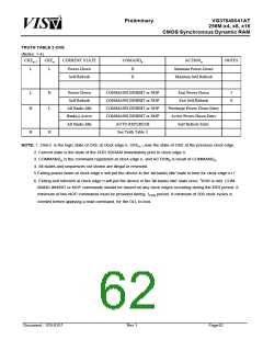
TRUTH TABLE 2-CKE
(Notes: 1-4)
CKEn-1
CKEn
L
CURRENT STATE
COMANDn
ACTIONn
NOTES
L
Power-Down
Self Refresh
X
X
Maintain Power-Down
Maintain Self Refresh
L
H
L
Power-Down
Self Refresh
COMMAND INHIBIT or NOP
COMMAND INHIBIT or NOP
COMMAND INHIBIT or NOP
COMMAND INHIBIT or NOP
AUTO REFERESH
Exit Power-Down
Exit Self Refresh
5
6
H
All Banks Idle
Bank(s) Active
All Banks Idle
Precharge Power-Down Entry
Active Power-Down Entry
Self Refresh Entry
H
H
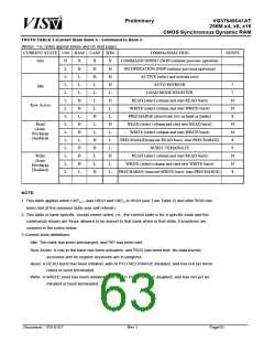
See Truth Table 3
NOTE: 1. CKEn is the logic state of CKE at clock edge n, CKEn-1 was the state of CKE at the previous clock edge.
2. Current state is the state of the DDR SDRAM immediately prior to clock edge n.
3. COMMANDn is the command registered at clock edge n, and ACTIONn is result of COMMANDn-
4. All states and sequences not shown are illegal or reserved.
5.Exiting power-down at clock edge n will put the device in the “all banks idle” state in time for clock edge n+1
t
6. Exiting self refreshh at clock edge n will put the device in the “all banks idle” state once XSR is met. COM-
MAND INHIBIT or NOP commands should be issued on any clock edges occurring during the X‘ SR period. A
minimum of two NOP commands must be provided during tXSR period. A minimum of 200 clock cycles is
needed before applying a read command, for the DLL to lock.
Document : 1G5-0157
Rev.1
Page62

 VML [ VANGUARD INTERNATIONAL SEMICONDUCTOR ]