Preliminary
VG37648041AT
256M:x4, x8, x16
VIS
CMOS Synchronous Dynamic RAM
T0
T1
T10
T2
T3
T4
T5
T6
T7
T9
T11
T8
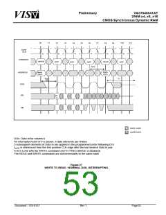
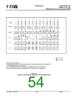
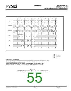
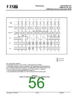
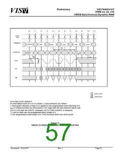
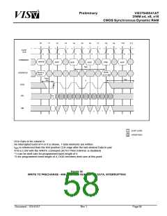
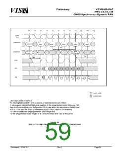
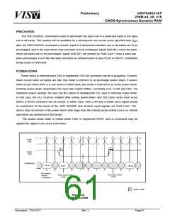
CLK#
CLK
COMMAND
ADDRESS
WRITE
NOP
PRE
NOP
NOP
NOP
tWR
Bank,
Bank a,
Col b
(a or all)
tDSS
min
tRP
*2
DQS
DQ
Dl
b
DM
*1
*1
*1
DONT’ CARE
UNDEFINED
Dl b=Data In for column b
An interrupted burst of 4 or 8 is shown, 2 data elements are written
1 subsequent element of Data In is applied in the programmed order following Dl b
tWR is referenced from the first positive CLK edge after the last desired Data In pair
A10 is LOW with the WRITE command (AUTO PRECHARGE is disabled)
*1=can be dont’ care for programmed burst length of 4
*2=for programmed burst length of 4, DQS becomes dont’ care at this point
Figure 31
WRITE TO PRECHARGE - MIN DSS, INTERRUPTING
Document : 1G5-0157
Rev.1
Page57

 VML [ VANGUARD INTERNATIONAL SEMICONDUCTOR ]