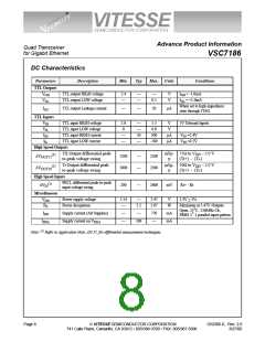
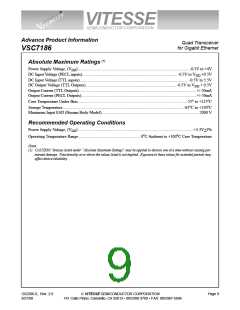
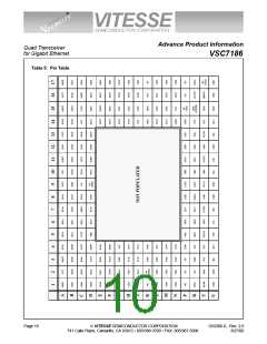
VITESSE
SEMICONDUCTOR CORPORATION
Advance Product Information
Quad Transceiver
for Gigabit Ethernet
VSC7186
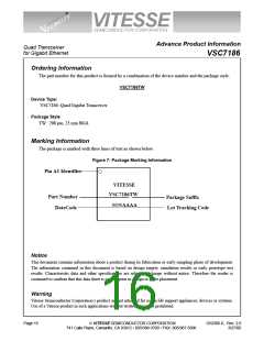
Pin
Name
Description
RX3-0, RX3-1,
RX3-2, RX3-3,
RX3-4, RX3-5,
RX3-6, RX3-7,
RX3-8, RX3-9
C17, D14, D15
D16, D17, E16
E17, F14, F15
F16
OUTPUT - TTL: 10-bit Receive bus for Channel 3. Parallel data on this bus
is synchronous to RC3-0 and RC3-1. RX3-0 is the first bit received.
INPUT - TTL: Recovered clock MODE control. When LOW, RCi0/RCi1 is
1/20th of the incoming baud rate. When HIGH, RCi0/RCi1 is 1/10th the
incoming baud rate.
T1
RCM0
OUTPUT - Complementary TTL: Recovered complementary clocks for
Channel 0 at 1/10th the incoming baud rate (RCM=HIGH) or 1/20th
(RCM=LOW). Synchronous to the RX0(0:9) bus and SYN0.
E1
E2
RC00
RC01
OUTPUT - Complementary TTL: Recovered complementary clocks for
Channel 1 at 1/10th the incoming baud rate (RCM=HIGH) or 1/20th
(RCM=LOW). Synchronous to the RX1(0:9) bus and SYN1.
A5
B5
RC10
RC11
OUTPUT - Complementary TTL: Recovered complementary clocks for
Channel 2 at 1/10th the incoming baud rate (RCM=HIGH) or 1/20th
(RCM=LOW). Synchronous to the RX20:9) bus and SYN2.
C10
D10
RC20
RC21
OUTPUT - Complementary TTL: Recovered complementary clocks for
Channel 3 at 1/10th the incoming baud rate (RCM=HIGH) or 1/20th
(RCM=LOW). Synchronous to the RX3(0:9) bus and SYN3.
B16
B17
RC30
RC31
U4, U3
U7, U6
U11, U10
U14, U13
SI0+, SI0-
SI1+, SI1-
SI2+, SI2-
SI3+, SI3-
INPUT - Differential PECL (AC Coupling recommended): Serial receive
data inputs for Channels 0-3 which are selected when LOOP is LOW.
[Internally biased to VDD/2]
INPUT - TTL: Parallel Loopback Enable input. SIi is input to the CRU for
Channel i (normal operation) when LOOP is LOW. When HIGH, internal
loopback paths from SOi to SIi are enabled.
N14
R17
LOOP
SYNC
INPUT - TTL: Enables SYNi and word alignment when HIGH. When LOW,
keeps current word alignment and disables SYNi (always LOW).
OUTPUT - TTL: Comma Detect for Channel i. This output goes HIGH for
half of an RCi1 period to indicate that RXi(0:9) contains a Comma Character
(‘0011111XXX’). SYNi will go HIGH only during a cycle when RCi0 is
rising. SYNi is enabled when SYNC is HIGH.
F2
A4
B10
B15
SYN0
SYN1
SYN2
SYN3
ANALOG: Loop Filter capacitor for the Clock Multiply Unit. Typically 0.1
uF connected between CAP0 and CAP1. Amplitude is less than 3.3V.
P9
R9
CAP0
CAP1
T17
D9
NC (TCK)
NC (TMS)
(INPUT - TTL: JTAG Test Clock)
(INPUT - TTL: JTAG Test Mode Select)
(INPUT - TTL: JTAG Test Reset, Active Low)
(INPUT - TTL: JTAG Test Data Input)
R15
P15
GND (TRSTN)
NC (TDI)
Page 12
VITESSE SEMICONDUCTOR CORPORATION
741 Calle Plano, Camarillo, CA 93012 • 805/388-3700 • FAX: 805/987-5896
G52306-0, Rev. 2.0
3/27/00

 VITESSE [ VITESSE SEMICONDUCTOR CORPORATION ]