VITESSE
SEMICONDUCTOR CORPORATION
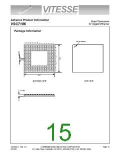
Advance Product Information
Quad Transceiver
for Gigabit Ethernet
VSC7186
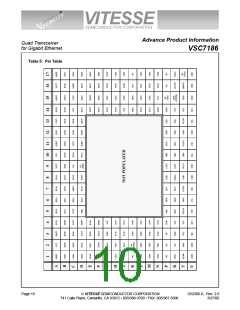
Table 6: Pin Description
Pin
Name
Description
TX0-0, TX0-1,
TX0-2 TX0-3,
TX0-4, TX0-5,
TX0-6, TX0-7,
TX0-8 TX0-9
N1, N2, N3
N4, M1, M2,
M3, M4, L1
L2
INPUT - TTL: 10-bit Transmit bus for Channel 0. Parallel data on this bus is
latched on the rising edge of REF. TX0-0 is transmitted first.
TX1-0, TX1-1,
TX1-2 TX1-3,
TX1-4, TX1-5,
TX1-6, TX1-7,
TX1-8, TX1-9
J1, J2, J3
J4, H1, H2
H3, H4, G1
G2
INPUT - TTL: 10-bit Transmit bus for Channel 1. Parallel data on this bus is
latched on the rising edge of REF. TX1-0 is transmitted first.
TX2-0, TX2-1,
TX2-2 TX2-3,
TX2-4, TX2-5,
TX2-6, TX2-7,
TX2-8, TX2-9
G16, G15, G14
H17, H16, H15
H14, J17, J16
J15
INPUT - TTL: 10-bit Transmit bus for Channel 2. Parallel data on this bus is
latched on the rising edge of REF. TX2-0 is transmitted first.
TX3-0, TX3-1,
TX3-2, TX3-3,
TX3-4, TX3-5,
TX3-6, TX3-7,
TX3-8, TX3-9
L17, L16, L15
L14, M17, M16
M15, M14, N17
N16
INPUT - TTL: 10-bit Transmit bus for Channel 3. Parallel data on this bus is
latched on the rising edge of REF. TX3-0 is transmitted first.
INPUT - TTL: TTL Reference clock. This rising edge of RFC1 provides the
reference clock, at 1/10th of the baud rate to the Clock Multiplying PLL. The
rising edge of RFC1 will latch TXi(0:9) on all four channels
R1
RFC1
R5, P5
R7, P7
P11, R11
P13, R13
SO0+, SO0-
SO1+, SO1-
SO2+, SO2-
SO3+, SO3-
OUTPUT - Differential PECL (AC Coupling recommended)
These pins output the serialized transmit data for Channels 0-3 when LOOP is
LOW. When LOOP is HIGH, SOi+ is HIGH and SOi- is LOW.
RX0-0, RX0-1,
RX0-2, RX0-3,
RX0-4, RX0-5,
RX0-6, RX0-7,
RX0-8, RX0-9
D1, D2, E3
E4, C1, C2
C3, B1, B2
B3
OUTPUT - TTL: 10-bit Receive bus for Channel 0. Parallel data on this bus is
synchronous to RC0-0 and RC0-1. RX0-0 is the first bit received.
RX1-0, RX1-1,
RX1-2, RX1-3,
RX1-4, RX1-5,
RX1-6, RX1-7,
RX1-8, RX1-9
A6, B6, C6
D6, A7, D7
A8, B8, C8
D8
OUTPUT - TTL: 10-bit Receive bus for Channel 1. Parallel data on this bus
is synchronous to RC1-0 and RC1-1. RX1-0 is the first bit received.
RX2-0, RX2-1,
RX2-2, RX2-3,
RX2-4, RX2-5,
RX2-6, RX2-7,
RX2-8, RX2-9
B11, A12, B12
C12, D12, B13
C13, D13, A14
B14
OUTPUT - TTL: 10-bit Receive bus for Channel 2. Parallel data on this bus
is synchronous to RC2-0 and RC2-1. RX2-0 is the first bit received.
G52306-0, Rev. 2.0
3/27/00
VITESSE SEMICONDUCTOR CORPORATION
741 Calle Plano, Camarillo, CA 93012 • 805/388-3700 • FAX: 805/987-5896
Page 11

 VITESSE [ VITESSE SEMICONDUCTOR CORPORATION ]