VSC6134
Datasheet
2.17.5
VSC6134 Clocking Structure
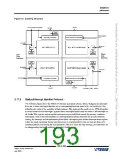
The clocking structure of the VSC6134 is shown in Figure 72, page 193. The loss of clock monitors are
also shown on the diagram. These monitors indicate that a clock is stuck high or low using a
microprocessor interrupt. For more information, see “Loss of Input Clock (LOCK) Monitor,” page 196.
To reduce the power dissipation of the VSC6134, it is possible to power down any combination of eight
clock domains through MPU control. The following domains may be powered down:
●
●
●
●
●
●
●
●
EFEC decoder DROP_EFEC_DEC_PWDN
Drop Reed Solomon decoder DROP_RS_DEC_PWDN
Add Reed Solomon decoder ADD_RS_DEC_PWDN
Drop Reed Solomon encoder DROP_RS_ENC_PWN
Add SDH block ADD_SONET_PWDN
Drop SDH block DROP_SONET_PWDN
Add 10GbE monitor ADD_ETHERNET_PWDN
Drop 10GbE monitor DROP_ETHERNET_PWDN
RXCLK0 and RXCLK1 are required in the drop and add paths respectively to detect LOS input signals
and LOF condition. Only corresponding TXCLKSRC0 and TXCLKSRC1 clocks are required to
manually force OTU_AIS, ODU-AIS, Generic AIS, or SONET L-AIS alarms. However, to
automatically generate ODU-AIS, Generic AIS, or SONET L-AIS alarms, RXCLK0 and RXCLK1 are
also required so that LOS/LOF condition can be detected. OTU-AIS cannot be generated automatically
(only manually).
Note: Microprocessor-accessible registers in clock domains that are not fed by their respective funtional
clocks (due to LOCK or power down) should not be read. This causes the microprocessor interface to
hang due to a lack of data acknowledge from the functional block.
2.17.6
JTAG Block Functional Description
The VSC6134 supports Boundary Scan according to the IEEE 1149.1 standard, using the JTAG
interface I/O. The Test Access Port (TAP) controller uses a standard five-pin serial interface. It supports
the instructions IDCODE, BYPASS, EXTEST and SAMPLE.
A single state machine controls the TAP controller. New TAP controller instructions are entered into the
shift register while the current instruction is stored in the instruction holding register. The shift is
performed on the rising edge of the TCK clock and the instruction holding register is updated on the
falling edge of the TCK clock. The instruction holding register is updated only while the TAP controller
state machine is in the Update-IR state.
197 of 438
VMDS-10185 Revision 4.0
July 2006

 VITESSE [ VITESSE SEMICONDUCTOR CORPORATION ]