VSC6134
Datasheet
2.17
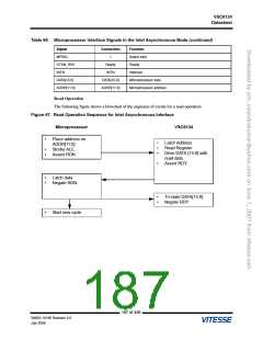
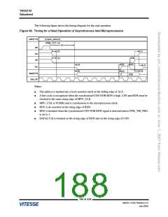
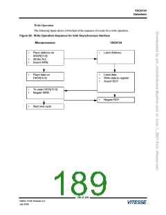
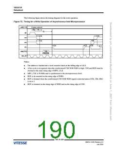
Special Topics
This section contains miscellaneous functional descriptions and special topics.
2.17.1
Device Initialization (Reset)
A hardware reset from pin HW_RESETN and a software reset from microprocessor configuration bit
SW_RESETN are combined for device initialization. Following a hardware or software reset, all on-
device flip-flops and memory blocks (for example, RAM) are initialized to known values. The memory
blocks are reset by writing zeros into them after the reset goes away. All blocks indicate proper
initialization using a BLOCK_RESET_RDY signal. All the BLOCK_RESET_RDY signals are
combined to generate a device RESET_RDY bit, indicating to the microprocessor that the device is
properly initialized and is ready to be configured.
A single reset generation module is used in every clock domain to synchronize the hardware and
software reset to the appropriate clock.
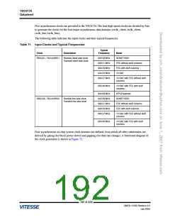
The reset block I/O is shown in the following table.
Table 70. Reset Block I/O Description
Name
Direction
Function
CLOCK
IN
IN
IN
The clock boundary to which the reset is synchronized.
An active low asynchronous hardware reset signal from the pin.
HW_RESETN
SW_RESETN
An active low asynchronous software reset signal, which is driven by a
register bit residing in the top microprocessor block.
RESETN
OUT
Active low rest signal for asynchronously resetting the flip-flops.
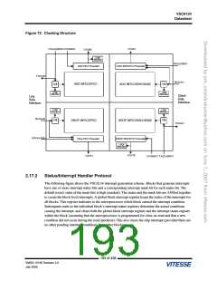
The following figure shows the block diagram of the reset module. When either HW_RESETN or
SW_RESETN are forced low, reset_n is asserted asynchronously. When both HW_RESETN and
SW_RESETN are forced high and de-asserted synchronously (subject to the two flip-flop delay), the
two staged flip-flops prevent metastability conditions and assure the synchronous de-assertion of
reset_n.
Figure 71. Reset Generation Module
.
HW_RESETN
1
reset_n
D Q
D Q
SW_RESETN
μp I/F
Clock
191 of 438
VMDS-10185 Revision 4.0
July 2006

 VITESSE [ VITESSE SEMICONDUCTOR CORPORATION ]