SFH617A
Optocoupler, Phototransistor Output,
High Reliability, 5300 VRMS, 110 °C Rated
Vishay Semiconductors
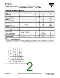
THERMAL CHARACTERISTICS (1)
PARAMETER
TEST CONDITION
at 25 °C
SYMBOL
Pdiss
Pdiss
Tjmax
Tjmax
θEB
VALUE
100
150
125
125
173
149
111
127
95
UNIT
mW
LED power dissipation
Output power dissipation
at 25 °C
mW
Maximum LED junction temperature
Maximum output die junction temperature
Thermal resistance, junction emitter to board
Thermal resistance, junction emitter to case
Thermal resistance, junction detector to board
Thermal resistance, junction detector to case
Thermal resistance, junction emitter to junction detector
Thermal resistance, board to ambient (2)
Thermal resistance, case to ambient (2)
°C
°C
°C/W
°C/W
°C/W
°C/W
°C/W
°C/W
°C/W
θEC
θDB
θDC
θED
θBA
195
3573
θCA
Notes
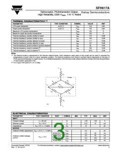
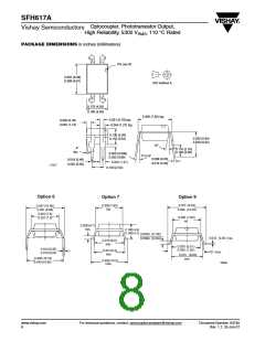
(1)
The thermal model is represented in the thermal network below. Each resistance value given in this model can be used to calculate the
temperatures at each node for a given operating condition. The thermal resistance from board to ambient will be dependent on the type of
PCB, layout and thickness of copper traces. For a detailed explanation of the thermal model, please reference Vishay's thermal characteristics
of optocouplers application note.
(2)
For 2 layer FR4 board (4" x 3" x 0.062).
TA
θ
CA
Package
TC
θ
EC
θ
DC
θ
TJE
TJD
DE
θ
DB
θ
EB
TB
θ
BA
19996
TA
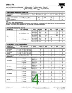
ELECTRICAL CHARACTERISTICS
PARAMETER
TEST CONDITION
PART
SYMBOL
MIN.
TYP.
MAX.
UNIT
INPUT
Forward voltage
Reverse current
Capacitance
IF = 60 mA
VF
IR
1.25
0.01
13
1.65
10
V
V
R = 6.0 V
µA
pF
V
R = 0 V, f = 1.0 MHz
CO
OUTPUT
Collector emitter capacitance
V
CE = 5.0 V, f = 1.0 MHz
VCE = 10 V
CCE
ICEO
ICEO
ICEO
ICEO
5.2
2.0
2.0
5.0
5.0
pF
nA
nA
nA
nA
SFH617A-1
SFH617A-2
SFH617A-3
SFH617A-4
50
50
Collector emitter leakage
current
100
100
Document Number: 83740
Rev. 1.7, 25-Jan-07
For technical questions, contact: optocoupler.answers@vishay.com
www.vishay.com
3

 VISHAY [ VISHAY ]