SFH617A
Optocoupler, Phototransistor Output,
High Reliability, 5300 VRMS, 110 °C Rated
Vishay Semiconductors
ABSOLUTE MAXIMUM RATINGS (1)
PARAMETER
TEST CONDITION
SYMBOL
VALUE
UNIT
INPUT
Reverse voltage
VR
IF
6.0
60
V
mA
DC forward current
Surge forward current
Derate linearly from 25 °C
OUTPUT
t ≤ 10 µs
IFSM
2.5
A
0.95
mW/°C
Collector emitter voltage
Emitter collector voltage
VCE
VEC
IC
70
7.0
V
V
50
mA
Collector current
t ≤ 1.0 ms
IC
100
1.54
mA
Derate linearly from 25 °C
mW/°C
COUPLER
Isolation test voltage
between emitter and detector, refer to
climate DIN 40046, part 2, Nov. 74
VISO
5300
VRMS
V
IO = 500 V, Tamb = 25 °C
RIO
RIO
≥ 1012
≥ 1011
Ω
Ω
Isolation resistance
V
IO = 500 V, Tamb = 100 °C
Storage temperature range
Ambient temperature range
Tstg
Tamb
- 55 to + 150
- 55 to + 110
°C
°C
max. 10 s, dip soldering distance
Soldering temperature (2)
Tsld
260
°C
to seating plane ≥ 1.5 mm
Notes
(1)
(2)
Tamb = 25 °C, unless otherwise specified.
Stresses in excess of the absolute maximum ratings can cause permanent damage to the device. Functional operation of the device is not
implied at these or any other conditions in excess of those given in the operational sections of this document. Exposure to absolute maximum
ratings for extended periods of the time can adversely affect reliability.
Refer to reflow profile for soldering conditions for surface mounted devices (SMD). Refer to wave profile for soldering conditions for through
hole devices (DIP).
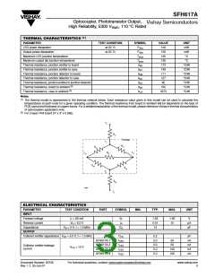
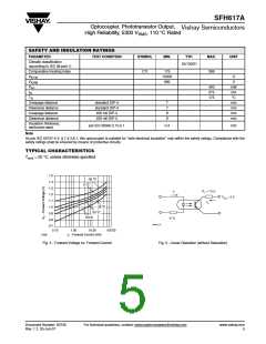
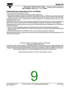
200
150
Detector
100
LED
50
0
0
20
40
60
80
100 120
T
amb
- Ambient Temperature (°C)
18778
Fig. 1 - Permissible Power Dissipation vs. Ambient Temperature
www.vishay.com
2
For technical questions, contact: optocoupler.answers@vishay.com
Document Number: 83740
Rev. 1.7, 25-Jan-07

 VISHAY [ VISHAY ]